Trench isolation for reduced cross talk

a cross-talk and isolation technology, applied in the direction of microstructural technology, electric devices, solid-state devices, etc., can solve the problems of amplifier oscillation, voltage differences at the rate of bits, and additional transient nois

Inactive Publication Date: 2009-12-10
SILEX MICROSYST
View PDF5 Cites 12 Cited by
  • Summary
  • Abstract
  • Description
  • Claims
  • Application Information

AI Technical Summary

Problems solved by technology

If this ground differs from the originator of the signal, this will cause voltage differences at the rate of the bits.
Some of the major problems induced by digital to analog and analog to analog cross talk are (1) high speed digital clocks cause severe interference with RF or IF front ends; (2) in digital portables, time-division-multiple-access (TDMA) may be used and power on/off cycles happen fairly frequently, causing additional transient noise on the power and ground planes; (3) in frequency division duplex systems, as well as in pixel based imaging devices, high-power transmit signals cause interference with

Method used


Image

  • Trench isolation for reduced cross talk
  • Trench isolation for reduced cross talk
  • Trench isolation for reduced cross talk

Examples


Embodiment Construction

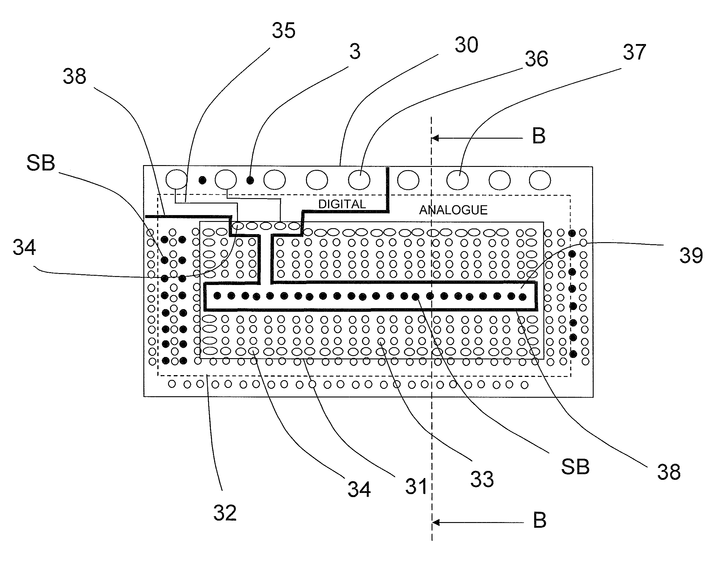
[0030]In the following description specific terms and expression will be given the following meanings:

[0031]Capactive crosstalk: when digital signals are run near analog signals, the capacitance between the lines can cause the lines to couple and the signals become blurred due to coupling through the substrate underneath. This problem can be eliminated by running the analog signals in a separate routing area than the digital, and by putting grounding shields between the analog and the digital.

[0032]The invention will now be further illustrated by embodiments thereof with reference to the drawings.

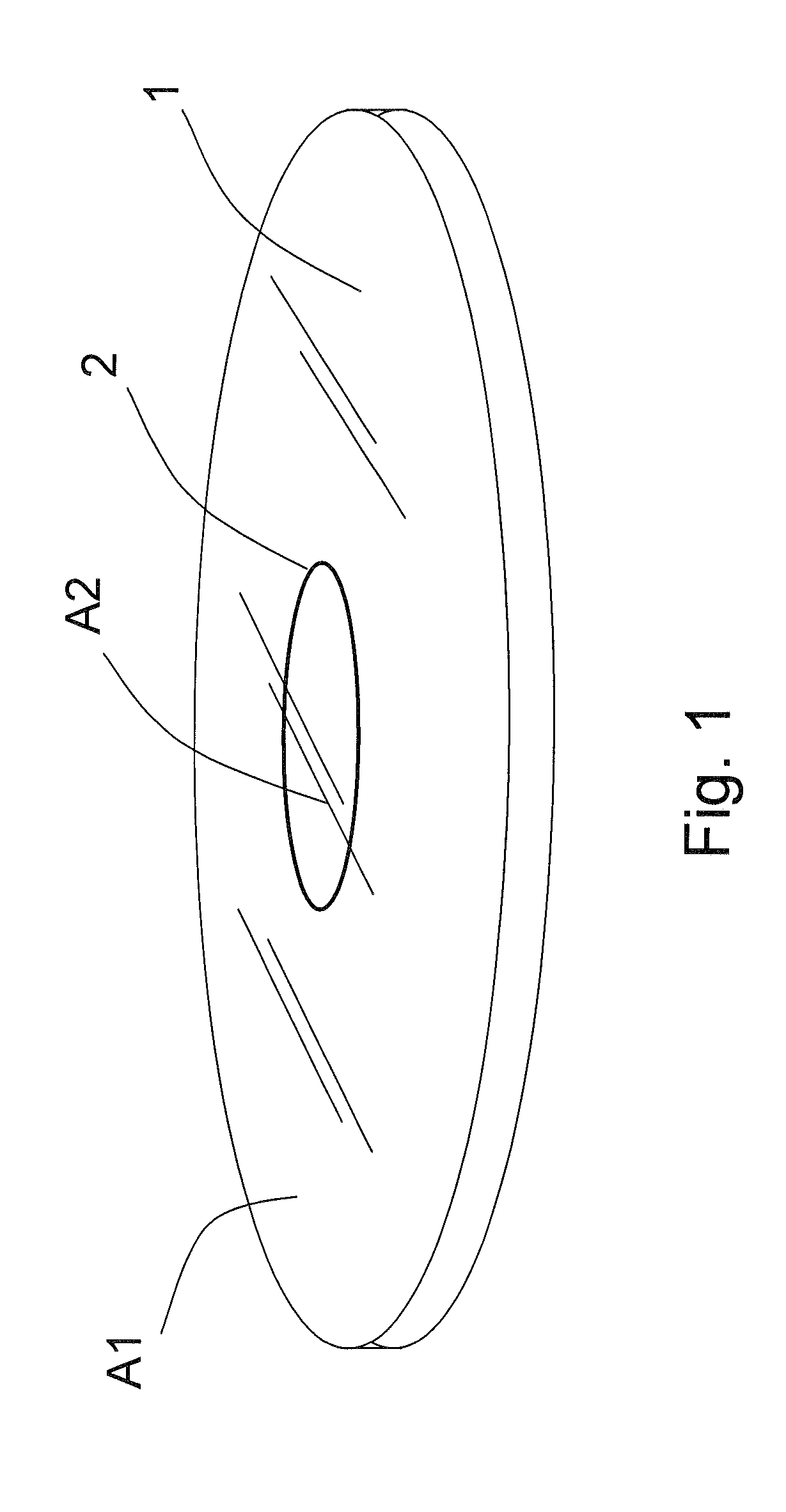
[0033]In its simplest embodiment the invention can be represented by the structure shown in FIG. 1. It comprises a wafer 1 of e.g. silicon, although a number of other semi-conductor materials are possible. The wafer has two areas A1 and A2, respectively, separated from each other by a barrier of insulating material 2 extending through the wafer and enclosing one area A2. The wafer should be...


PUM


Abstract

A starting substrate in the form of a semiconductor wafer (1) has a first side and a second side, the sides being plane-parallel with respect to each other, and has a thickness rendering it suitable for processing without significant risk of being damaged, for the fabrication of combined analogue and digital designs, the wafer including at least two partitions (A1, A2; DIGITAL, ANALOGUE) electrically insulated from each other by insulating material (2; 38; 81; L) extending entirely through the wafer. A method for making such substrates including etching trenches in a wafer, and filling trenches with insulating material is also described.

Description

FIELD OF THE INVENTION[0001]The present invention relates to design of micro electronic devices where e.g. both analogue and digital units are to be located in close proximity on substrates such as micro chips. In particular it relates to means and methods for eliminating or at least reducing so called cross-talk between analogue / digital components on the same substrate.BACKGROUND OF THE INVENTION[0002]When analogue and digital components are located on the same substrate in close proximity, such as is the case for ASIC devices, inevitably there will occur so called cross-talk between these components.[0003]Capactive crosstalk can e.g. occur when digital signals are run near analog signals, the capacitance between the lines can cause the lines to couple and the signals become blurred due to coupling through the substrate underneath.[0004]This problem can be eliminated by running the analog signals in a separate routing area than the digital, and by putting grounding shields between ...

Claims


Application Information

Patent Timeline
IPC IPC(8): H01L29/06H01L21/762H10K39/10H10K59/90
CPCH01L21/762H01L21/823481H01L2924/1461H01L23/147H01L23/055H01L23/49838H01L23/552H01L23/66H01L2223/6622H01L2223/6688H01L2924/09701H01L2924/1433H01L2924/3011H01L2224/16225H01L2924/01322B81C1/00246H01L2924/00H01L2924/00014H01L23/26H01L2224/16235H01L2924/15153H01L2924/16195H01L2924/16251H01L2924/00011H01L2224/0401B81B7/0077B81C3/008H01L23/04H01L23/06H01L25/10
Inventor EBEFORS, THORBJORNBAUER, TOMAS
Owner SILEX MICROSYST
Why Eureka
Try Eureka