Through Substrate Via Semiconductor Components

Active Publication Date: 2009-12-10
INFINEON TECH AG
View PDF15 Cites 74 Cited by
  • Summary
  • Abstract
  • Description
  • Claims
  • Application Information

AI Technical Summary

Benefits of technology

[0006]These and other problems are generally solved or circumvented, and technical advantages are generally achie

Problems solved by technology

However, introduction of such interconne

Method used


Image

  • Through Substrate Via Semiconductor Components
  • Through Substrate Via Semiconductor Components
  • Through Substrate Via Semiconductor Components

Examples


Embodiment Construction

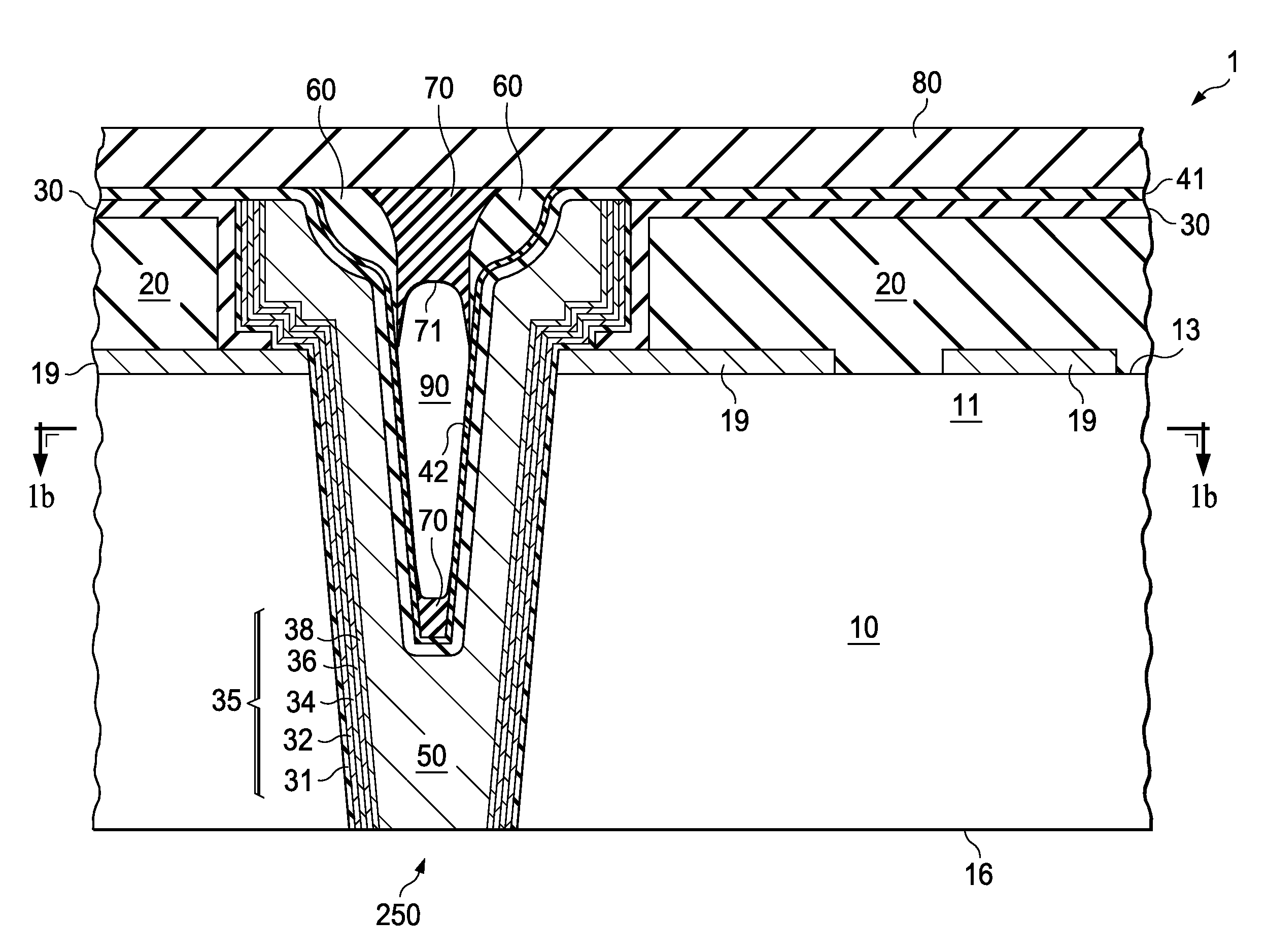
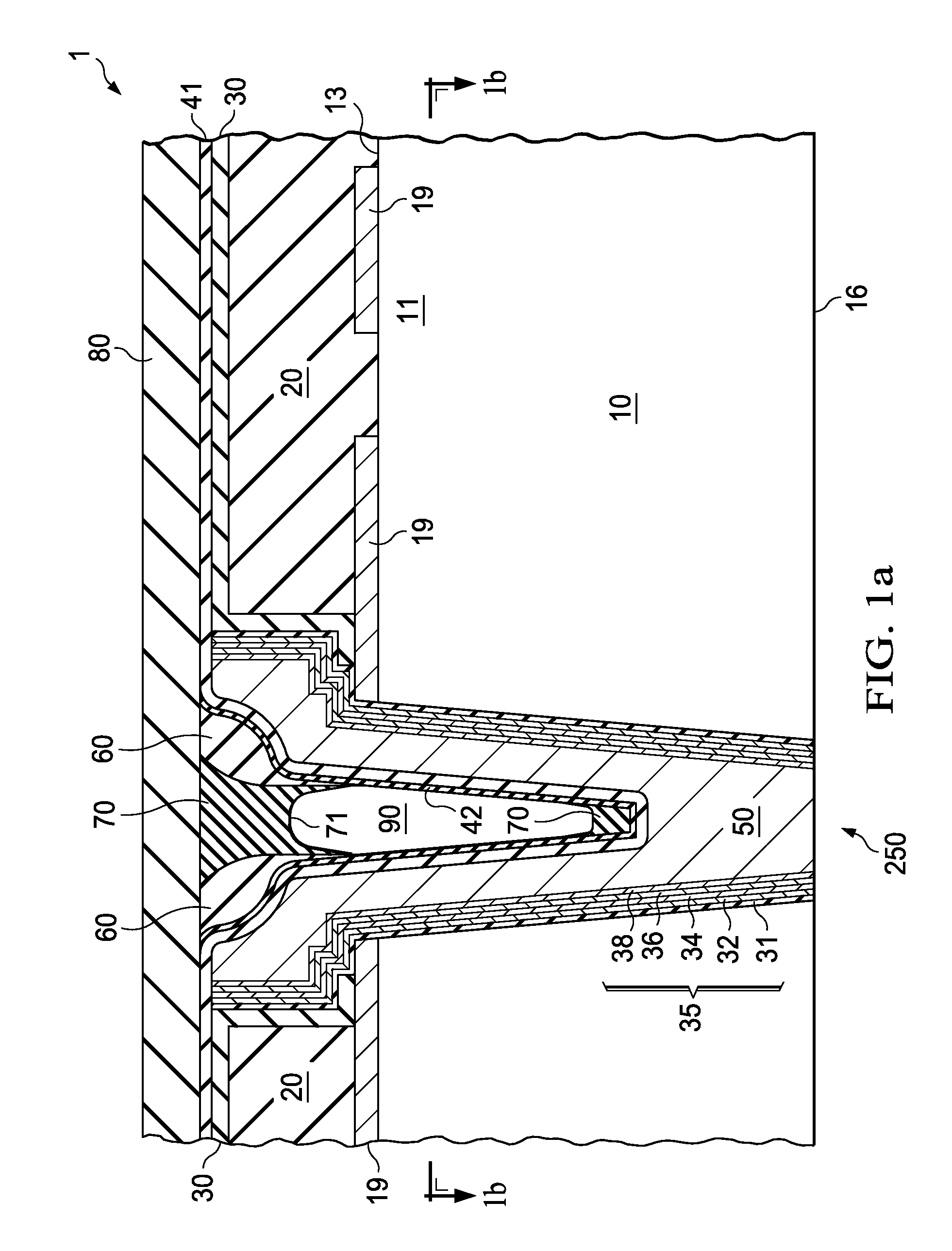
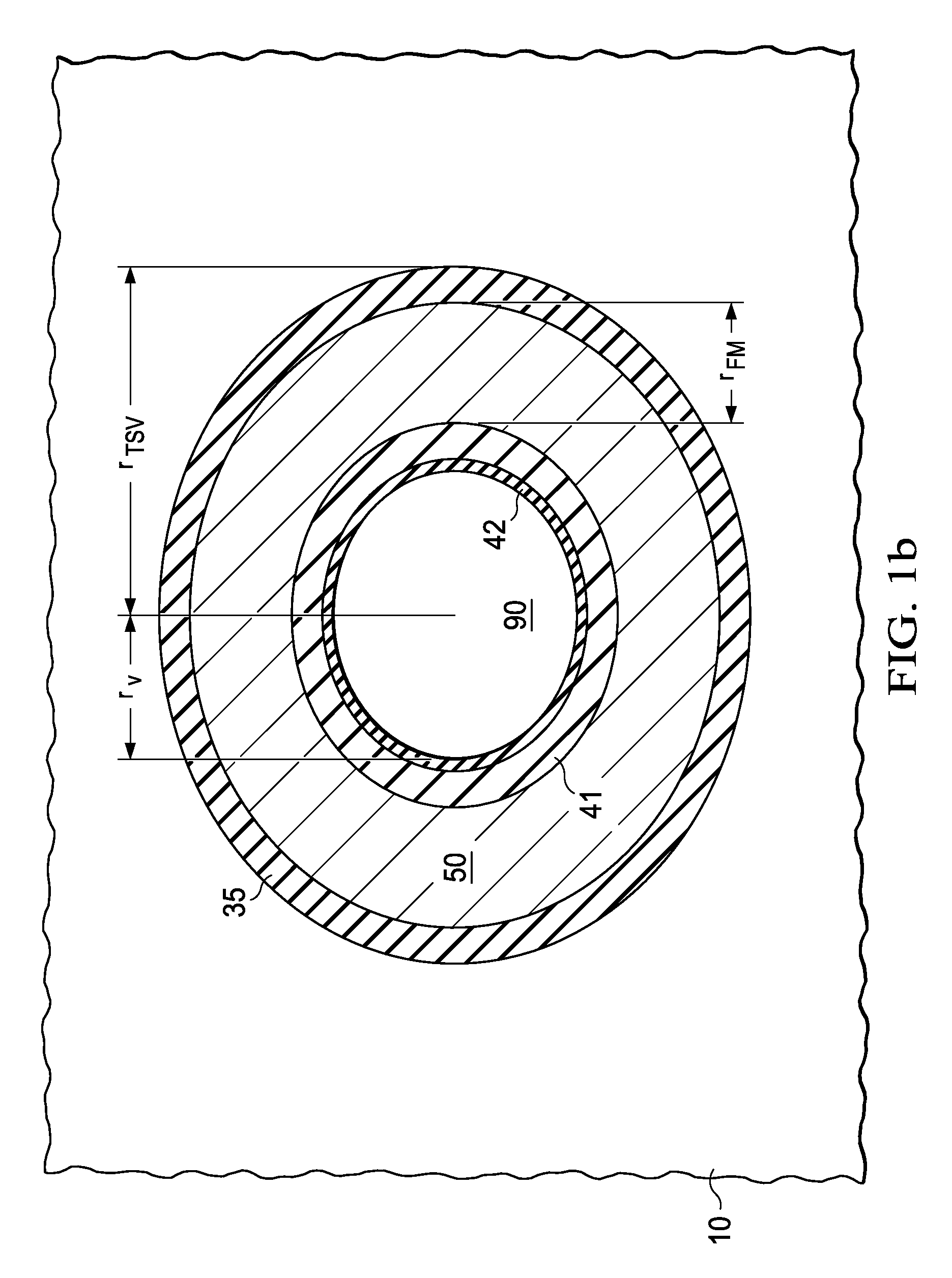
[0019]The making and using of the presently preferred embodiments are discussed in detail below. It should be appreciated, however, that the present invention provides many applicable inventive concepts that can be embodied in a wide variety of specific contexts. The specific embodiments discussed are merely illustrative of specific ways to make and use the invention, and do not limit the scope of the invention.

[0020]The present invention will be described with respect to preferred embodiments in a specific context, namely partially filled through substrate vias. The invention may also be applied, however, to other semiconductor components comprising, for example, multiple chips and / or in forming voids or micro-voids in other components. One of ordinary skill in the art will be able to recognize further examples as well.

[0021]Embodiments of the present invention utilize through substrate vias to create 3D chip packages. Stacking chips on top of one another provides a means to achiev...


PUM


Abstract

A structure and method of forming through substrate vias in forming semiconductor components are described. In one embodiment, the invention describes a method of forming a through substrate via by partially filling an opening with a fill material, and forming a first insulating layer over the first fill material thereby forming a gap over the opening. The method further includes forming a second insulating layer to close the gap thereby forming an enclosed cavity within the opening.

Description

TECHNICAL FIELD[0001]This invention relates generally to electronic devices, and more particularly to through substrate via semiconductor components.BACKGROUND[0002]One of the goals in the fabrication of electronic components is to minimize the size of various components. For example, it is desirable that hand held devices such as cellular telephones and personal digital assistants (PDAs) be as small as possible. To achieve this goal, the semiconductor circuits that are included within the devices should be as small as possible. One way of making these circuits smaller is to stack the chips that carry the circuits.[0003]A number of ways of interconnecting the chips within the stack are known. For example, bond pads formed at the surface of each chip can be wire-bonded, either to a common substrate or to other chips in the stack. Another example is a so-called micro-bump 3D package, where each chip includes a number of micro-bumps that are routed to a circuit board, e.g., along an ou...

Claims


Application Information

Patent Timeline
IPC IPC(8): H01L23/48H01L21/31
CPCH01L21/76898H01L23/481H01L2924/0002H01L2924/00014H01L2224/05571H01L2224/0557H01L2224/04042H01L2224/13009H01L2224/13025H01L2224/16H01L2924/01079H01L2924/01019H01L2924/01068H01L21/76877H01L2224/0401H01L2924/00012H01L2224/05552
Inventor BIRNER, ALBERTHOECKELE, UWEKUNSTMANN, THOMASSEIDEL, UWE
Owner INFINEON TECH AG
Why Eureka
Try Eureka