Process sequence for doped silicon fill of deep trenches

a technology of deep trenches and process sequences, which is applied in the direction of coatings, chemical vapor deposition coatings, solid-state devices, etc., can solve the problems of slow deposition rate, high deposition rate within the trench relative to the surface, and short residence time of gases on the wafer surface, etc., and achieves the effect of high deposition ra

Inactive Publication Date: 2006-06-15
APPLIED MATERIALS INC
View PDF7 Cites 21 Cited by
  • Summary
  • Abstract
  • Description
  • Claims
  • Application Information

AI Technical Summary

Benefits of technology

[0015] The present invention relates generally to a “super-fill” process, and relies on the fact that a different partial pressure and residence time can be achieved for points on the surface of the wafer compared to within the trench by appropriately modulating the gas flow rates and chamber pressure. If the arsine concentration is higher and the gas residence time is shorter at the surface of the trench relative to a point within the trench, the resulting poisoning effect results in a higher deposition rate within the trench relative to the surface. Thus the key is to achieve differential concentrations and gas residence times within the trench relative to the surface.

Problems solved by technology

If the arsine concentration is higher and the gas residence time is shorter at the surface of the trench relative to a point within the trench, the resulting poisoning effect results in a higher deposition rate within the trench relative to the surface.
The high total flow results in a short residence time of gases on the wafer surface.
This results in a slow deposition rate and high As concentration at the top of the trench.
The high concentration of SiH4 in the trench and the high total pressure results in a high rate of SiH2 formation inside the trench while the low diffusivity of AsH3 in the trench, reduces the surface poisoning effect.

Method used


Image

  • Process sequence for doped silicon fill of deep trenches
  • Process sequence for doped silicon fill of deep trenches
  • Process sequence for doped silicon fill of deep trenches

Examples


Embodiment Construction

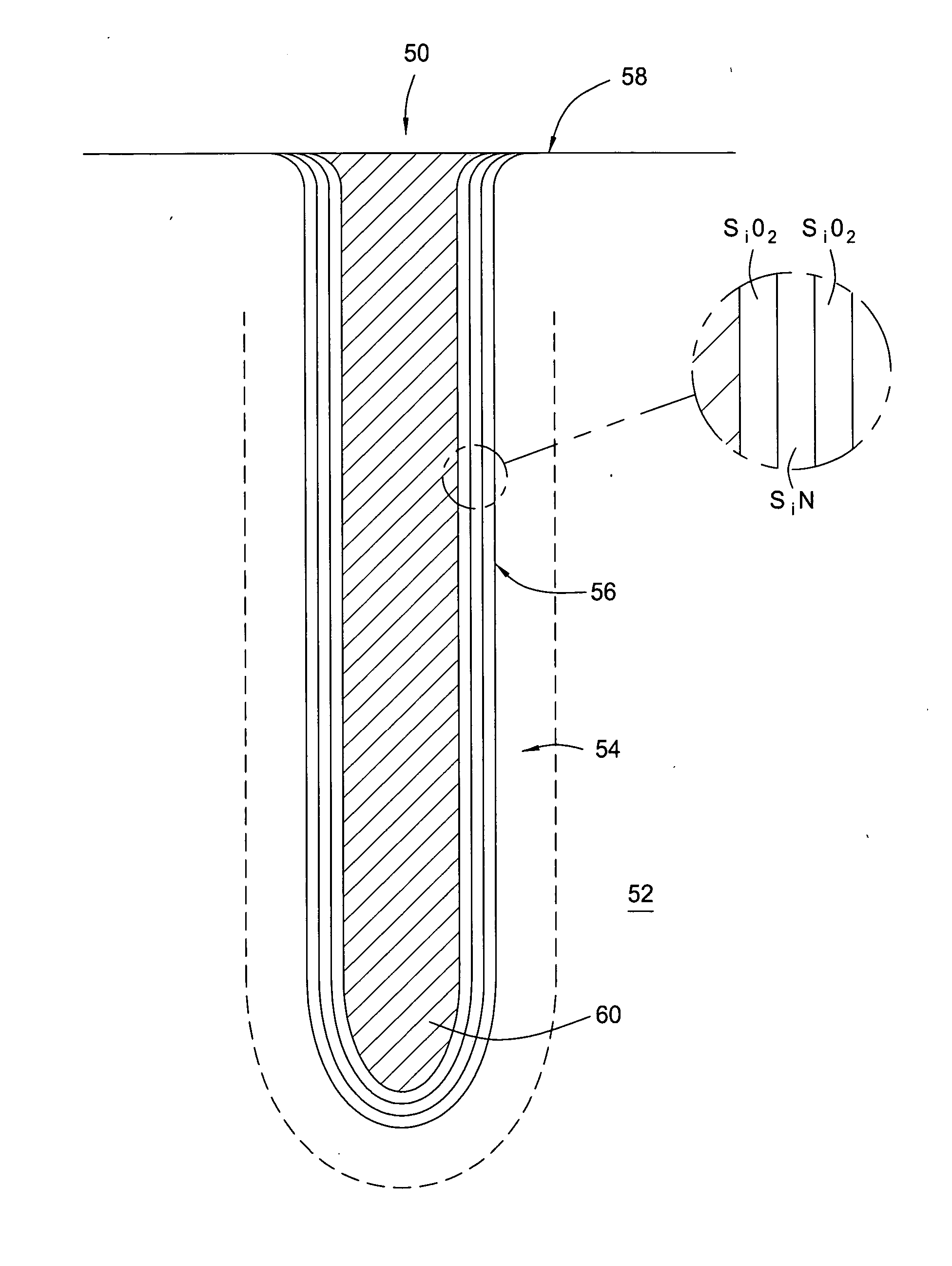
[0034] By way of the present invention it is possible to fill deep trenches with in-situ doped amorphous silicon, and particularly As doped amorphous silicon films, without the formation of voids, while at the same time producing deposited films of high quality, having a step coverage of greater than 100%, and as much as 150%, a WIW (With In Wafer) non uniformity of 20 / cm3. In addition, in the case of multiple wafer processing, such as is achievable in the FlexStar chamber, hereinafter described, as many as 26-51 wafers can be processed at once.

[0035] In the fabrication of deep trench capacitor structures, trenches of high aspect ratio are first formed in single crystal wafers, such trenches having aspect ratios of 25-50:1 or greater, such as may be required for ever smaller critical dimension structures. With reference to FIGS. 4 and 5, in order to provide for a void free trench fill, the filling sequence is carried out in a number of separate steps. To start, a partially processe...


PUM

PropertyMeasurementUnit
temperatureaaaaaaaaaa
pressureaaaaaaaaaa
temperatureaaaaaaaaaa

Abstract

A method for void free filling with in-situ doped amorphous silicon of a deep trench structure is provided in which a first fill is carried out in at a temperature, pressure and dopant to silane ratio such that film deposition occurs from the bottom of the trench upwards. By way of this first fill, step coverages well in excess 100% are achieved. In the second fill step, deposition is carried out under changed conditions so as to reduce the impact of dopant on deposition rate, whereby trench fill is completed at a deposition rate which exceeds the deposition rate of the first fill. In an application of this method to the formation of deep trench capacitor structures, the intermediate steps further including the capping of the void free filled trench with a thick layer of amorphous silicon, planarization of the wafer thereafter, followed by a thermal anneal to re-distribute the dopant within the filled trench. Thereafter, additional steps can be performed to complete the formation of the capacitor structure.

Description

FIELD OF THE INVENTION [0001] Embodiments of the present invention relate generally to a method for filling of deep trenches with low resistivity, doped α-silicon films in connection with the fabrication of deep trench capacitors. More particularly the invention deals with a sequential method for the void-free filling of said deep trench structures with in-situ doped α-silicon. A further feature of the invention is the providing of a production worthy approach for in-situ doped silicon films using a parallel wafer processing reactor. DESCRIPTION OF THE RELATED ART [0002] Arsenic-doped α-silicon films with As concentrations ranging from 1020 / cm3 to 1021 / cm3 are used in a variety of semiconductor device applications. These include word lines, bit lines, landing pads, storage node / bit line contact plugs, gate electrodes in ROM devices, as well as floating gate electrode / control gate electrodes in non-volatile memory devices. It is preferred in connection with the fabrication of such st...

Claims


Application Information

Patent Timeline
Patent Type & Authority Applications(United States)
IPC IPC(8): H01L21/4763
CPCC23C16/045C23C16/24H01L21/76232H01L29/66181H01L21/205H01L21/4763H01L27/04H10B12/00
Inventor PARANJPE, AJITNAG, SOMNATH
Owner APPLIED MATERIALS INC
Why Eureka
Try Eureka