Organic light emitting display device and method of manufacturing the same

Inactive Publication Date: 2009-12-10
SAMSUNG DISPLAY CO LTD
View PDF0 Cites 3 Cited by
  • Summary
  • Abstract
  • Description
  • Claims
  • Application Information

AI Technical Summary

Benefits of technology

[0021]According to another aspect of the present invention, there is provided an organic light emitting display device comprising: a substrate; an organic light emitting unit formed on the substrate; a sealing unit sealing the organic light emitting unit; a pro

Problems solved by technology

The OLED is easily damaged by materials such as moisture or oxygen if they penetrate

Method used


Image

  • Organic light emitting display device and method of manufacturing the same
  • Organic light emitting display device and method of manufacturing the same
  • Organic light emitting display device and method of manufacturing the same

Examples


Example

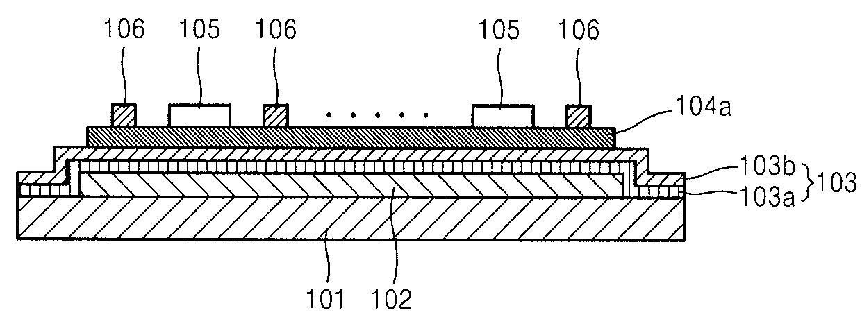
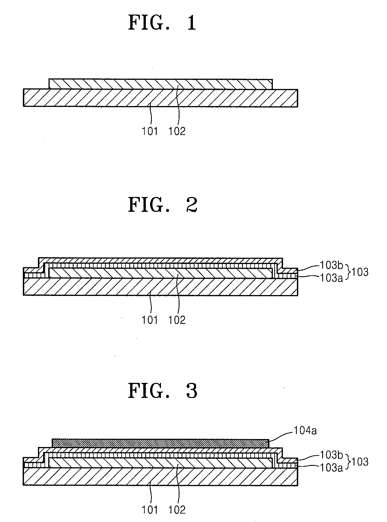
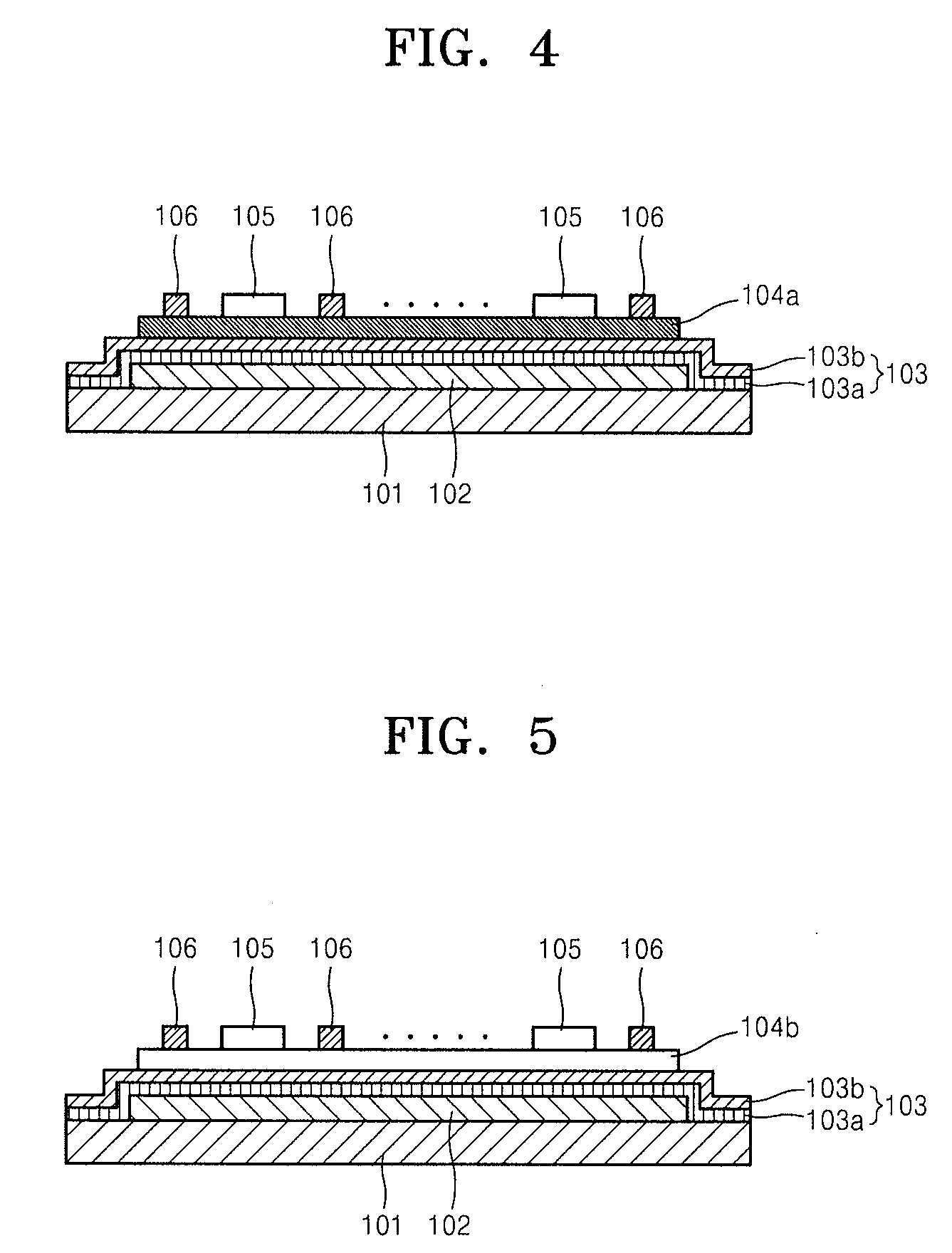
[0032]The present invention will now be described more fully with reference to the accompanying drawings, in which exemplary embodiments of the invention are shown. The invention may, however, be embodied in many different forms and should not be construed as being limited to the embodiments set forth herein; rather, these embodiments are provided so that this disclosure will be thorough and complete, and will fully convey the concept of the invention to those skilled in the art. In the drawings, the thicknesses of layers and regions are exaggerated for clarity. Like reference numerals in the drawings denote like elements.

[0033]FIGS. 1 through 5 are cross-sectional views illustrating a method of manufacturing an organic light emitting display device according to an embodiment of the present invention.

[0034]Referring to FIG. 1, an organic light emitting unit 102 is formed on a substrate 101.

[0035]The substrate 101 can be formed of a material such as transparent glass, plastic sheet, ...


PUM


Abstract

Provided is a method of manufacturing an organic light emitting display device in which a laser beam is used. The method includes forming an organic light emitting unit on a substrate; forming a sealing unit that seals the organic light emitting unit; forming an protective film which is opaque on the sealing unit to protect the organic light emitting unit or the sealing unit by blocking the transmission of the laser beam; forming an optical pattern on the opaque protective film using the laser beam; and forming a transparent film from the opaque protective film by oxidizing the opaque protective film.

Description

CROSS-REFERENCE TO RELATED PATENT APPLICATION[0001]This application claims the benefit of Korean Patent Application No. 10-2008-0054301, filed on Jun. 10, 2008, in the Korean Intellectual Property Office, the disclosure of which is incorporated herein in its entirety by reference.BACKGROUND OF THE INVENTION[0002]1. Field of the Invention[0003]The present invention relates to an organic light emitting display device and a method of manufacturing the same, and more particularly, to an organic light emitting display device that can prevent the organic light emitting display device from being damaged by a laser which is used in the manufacturing process and a method of manufacturing the same.[0004]2. Description of the Related Art[0005]Generally, flat panel display (FPD) devices can be classified into devices that use inorganic material and devices that use organic material. Devices that use inorganic material include plasma display panels (PDPs) that use photo luminescence (PL) and fie...

Claims


Application Information

Patent Timeline
IPC IPC(8): H01L51/54H01L51/56
CPCH01L27/322H01L51/5284H01L51/5237H10K59/38H10K50/844H10K50/865H01L33/42H01L33/52H10K10/476H10K50/84
Inventor KWACK, JIN-HOSUH, MIN-CHULLEE, JAE-HO
Owner SAMSUNG DISPLAY CO LTD
Why Eureka
Try Eureka