Solid-state image pickup device and camera
a pickup device and solid-state technology, applied in the field of solid-state image pickup devices, can solve the problem of increasing the size of the adder circuit, and achieve the effect of suppressing random noise of the photoreceiving elements
- Summary
- Abstract
- Description
- Claims
- Application Information
AI Technical Summary
Benefits of technology
Problems solved by technology
Method used
Image
Examples
reference example 1
[0032]FIG. 7 shows the first reference example regarding the invention. This reference example shows an example of a case of executing a signal addition (averaging) of (3 pixels in the horizontal direction)×(3 pixels in the vertical direction) in a pixel array of (H columns×V rows).
[0033]In FIG. 7, reference numerals 101-a to 101-i denote photoreceiving elements which are two-dimensionally arranged. Reference numerals 112 to 114 denote vertical output lines to which a photoreceiving element train constructed by the photoreceiving elements 101-a, 101-d, and 101-g, a photoreceiving element train constructed by the photoreceiving elements 101-b, 101-e, and 101-h, and a photoreceiving element train constructed by the photoreceiving elements 101-c, 101-f, and 101-i are connected, respectively. Reference numerals 102-a to 102-c denote clamp capacitors in which one terminal is connected to the vertical output lines 112 to 114 and the other terminals are connected in common. Signals of the ...
reference example 2
[0041]FIG. 10 shows the second reference example of the invention. This reference example shows an example of a case of executing a signal addition of (3 pixels in the horizontal direction)×(4 pixels in the vertical direction) in a pixel array of (H columns×V rows).
[0042]In FIG. 10, reference numerals 401-a to 401-P denote photoreceiving elements which are two-dimensionally arranged. Reference numerals 413 to 415 denote vertical output lines. Reference numerals 402-a to 402-c denote clamp capacitors. The signal addition in the horizontal direction is executed by using those capacitors. Reference numeral 403 denotes an MOS switch for clamping which is connected to the clamp voltage Vclmp; 410 a common line for averaging outputs after the clamping; and 404 to 407 MOS switches for selecting the S / H capacitors. The MOS switches 404 to 407 are used to select the S / H capacitors. Reference numerals 408-a to 408-d denote sampling and holding capacitors and 409-a to 409-d indicate MOS switch...
embodiment 1
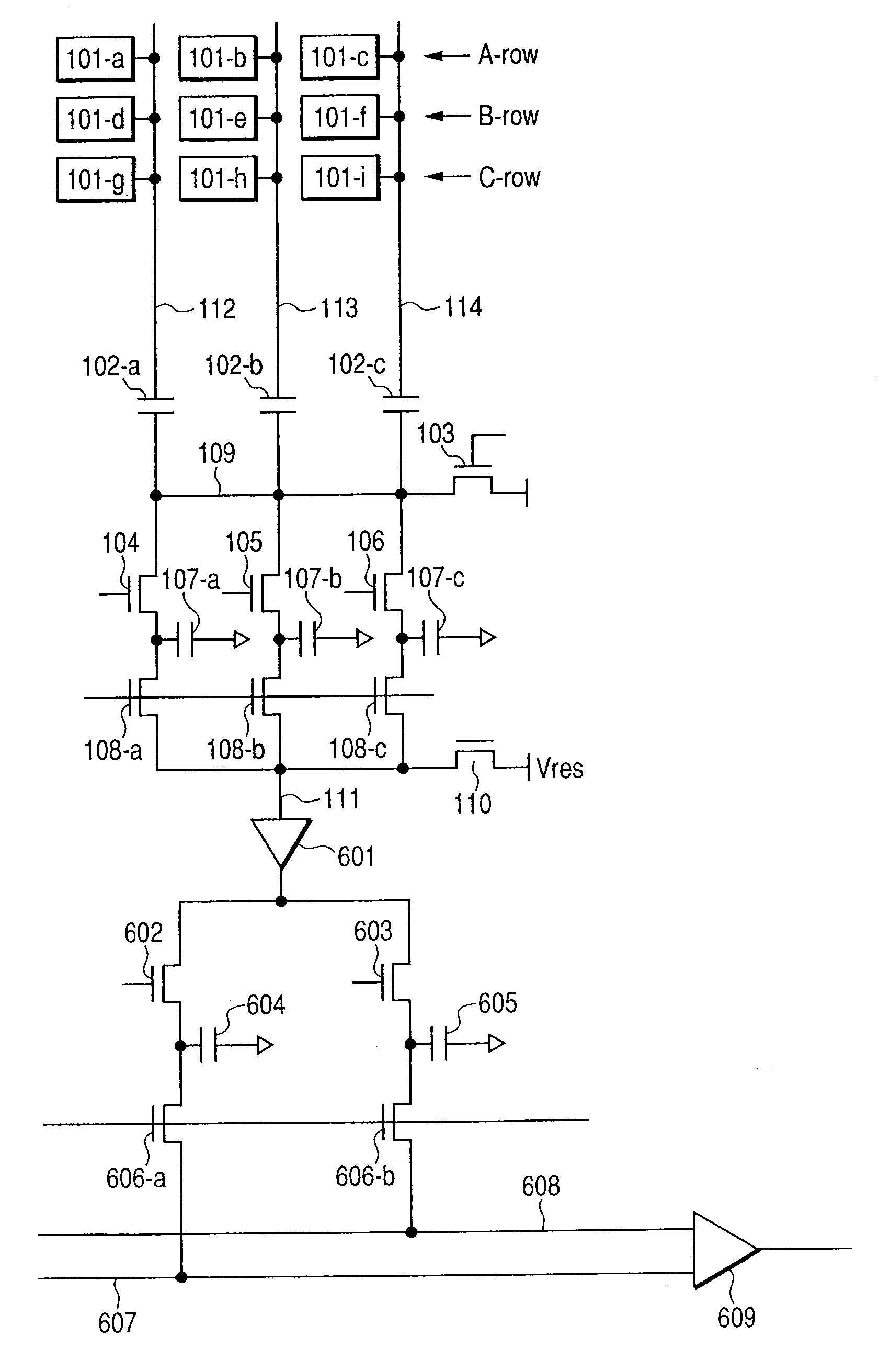
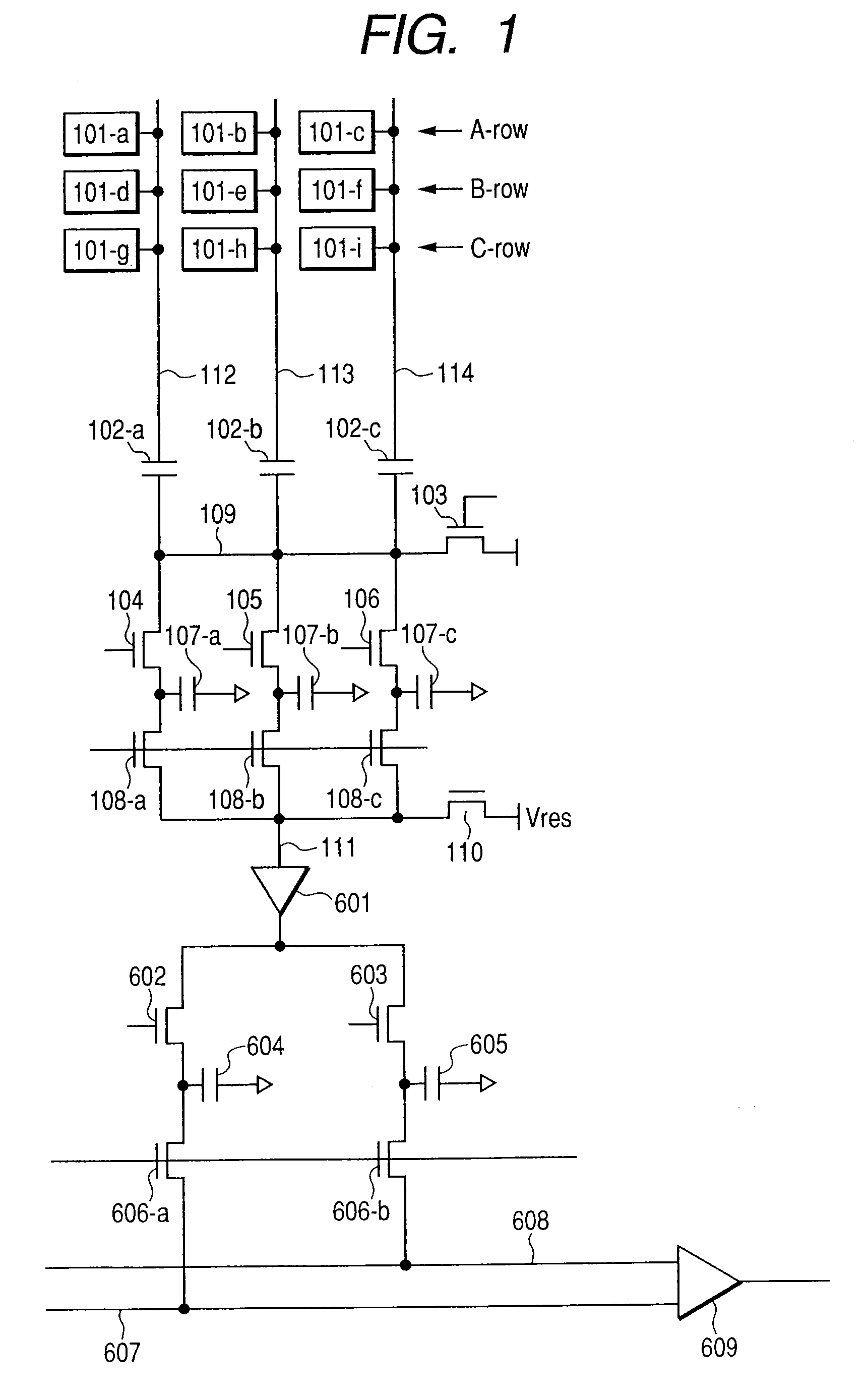
[0048]FIG. 1 shows the first embodiment according to the invention. This embodiment shows an example of the case of executing the addition of signals of (3 pixels in the horizontal direction)×(3 pixels in the vertical direction) in the pixel array of (H columns×V rows). By using this embodiment, loss of the signal components can be reduced more than that in the reference example 1. The same or similar component elements as those shown in FIG. 7 are designated by the same reference numerals and their description is omitted. Naturally, a construction of the embodiment can be also applied to the case of executing the addition of signals of (3 pixels in the horizontal direction)×(4 pixels in the vertical direction) in the pixel array of (H columns×V rows).
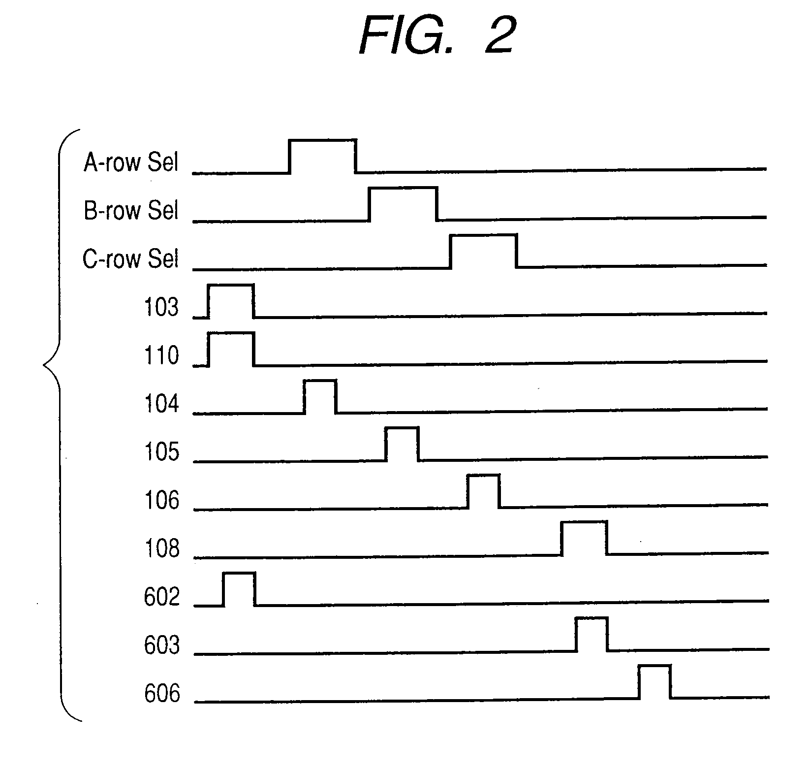
[0049]In FIG. 1, reference numeral 601 denotes a source follower amplifier; 602, 603, 606-a, and 606-b MOS switches; and 604 and 605 line memories. By turning on the MOS switch 602, a noise signal (containing an offset of the source fo...
PUM
 Abstract
Description
Claims
Application Information


