Non-volatile memory control circuit

a control circuit and non-volatile technology, applied in static storage, digital storage, instruments, etc., can solve the problems of affecting the operation of the program, the entire sector must be erased, and the data cannot be normally retrieved during the read operation, etc., to achieve effective erasure

Active Publication Date: 2009-12-10
SEMICON COMPONENTS IND LLC
View PDF3 Cites 0 Cited by
  • Summary
  • Abstract
  • Description
  • Claims
  • Application Information

AI Technical Summary

Benefits of technology

[0011]The present invention relates to a non-volatile memory control circuit for controlling erasure of non-volatile memory where source line voltage is manipulated in units of a sector composed of a predetermined plurality of memory cells. An erase command is received for memory cells to be erased of one or a plurality of word line units arranged within a sector, all data within the sector including the desired area to be erased is saved to another memory, erasure is performed for the entire sector, and among the saved data, the data of the memory cells not of the desired area to be erased is returned to the corresponding memory cells. Therefore, with the erase unit as the memory cell unit in common with word line, an effective erasure can be performed.

Problems solved by technology

Since the high voltage is also applied to memory cells that are not to be programmed, electrons enter the floating gate (FG) in accordance with the total application time of the high voltage and may cause a transfer to a program state, namely, a program disturb may occur, such as due to reverse tunneling phenomenon.
When the program disturb occurs, data cannot be normally retrieved during read operations.
Here a sector is a relatively large unit resulting in a problem where an entire sector must be erased and a large amount of data must be exchanged to rewrite data even when it is desirable to erase only a small amount of data.

Method used


Image

  • Non-volatile memory control circuit
  • Non-volatile memory control circuit
  • Non-volatile memory control circuit

Examples


Embodiment Construction

[0016]Embodiments of the present invention will be described hereinafter with reference to the attached drawings.

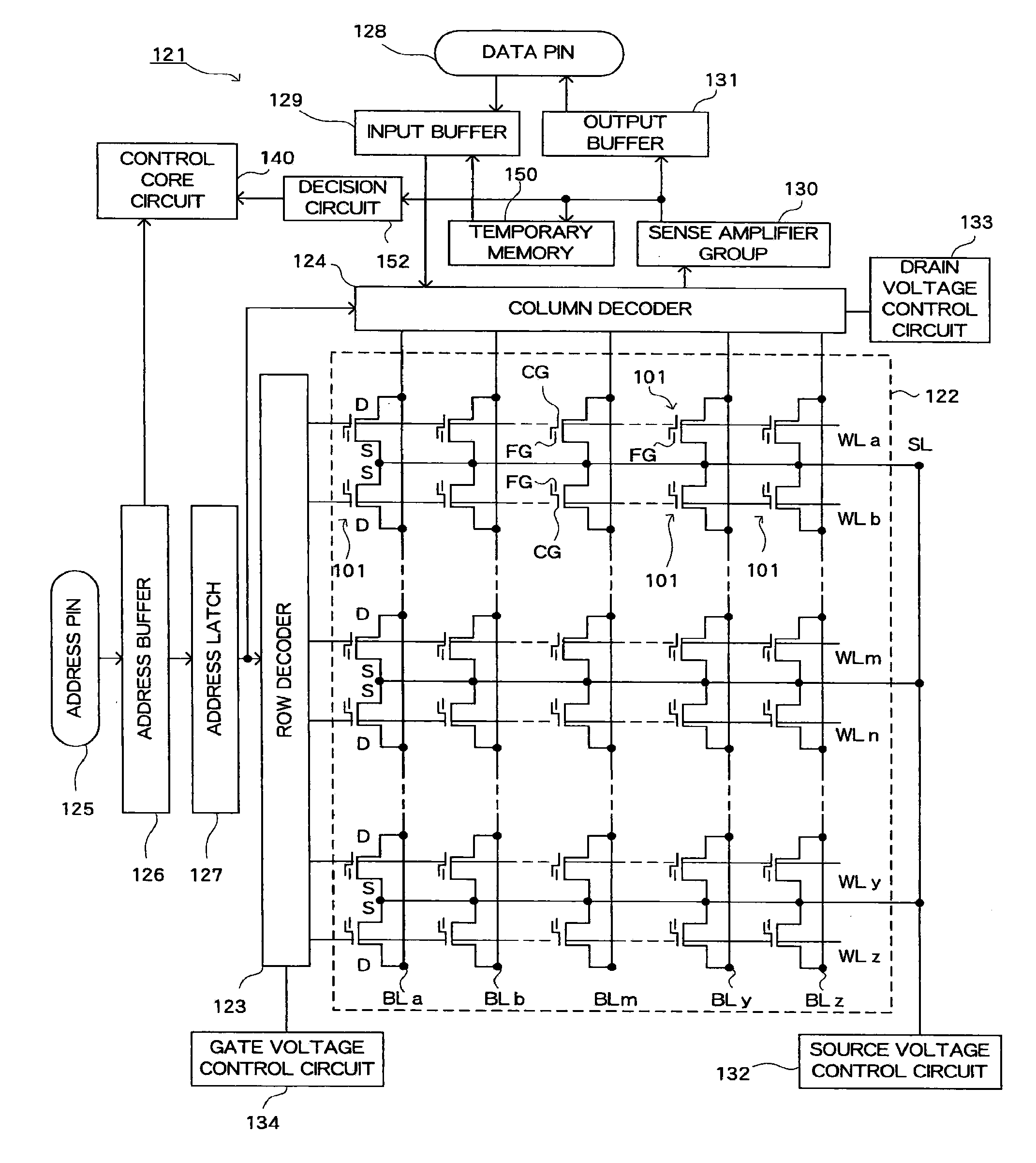
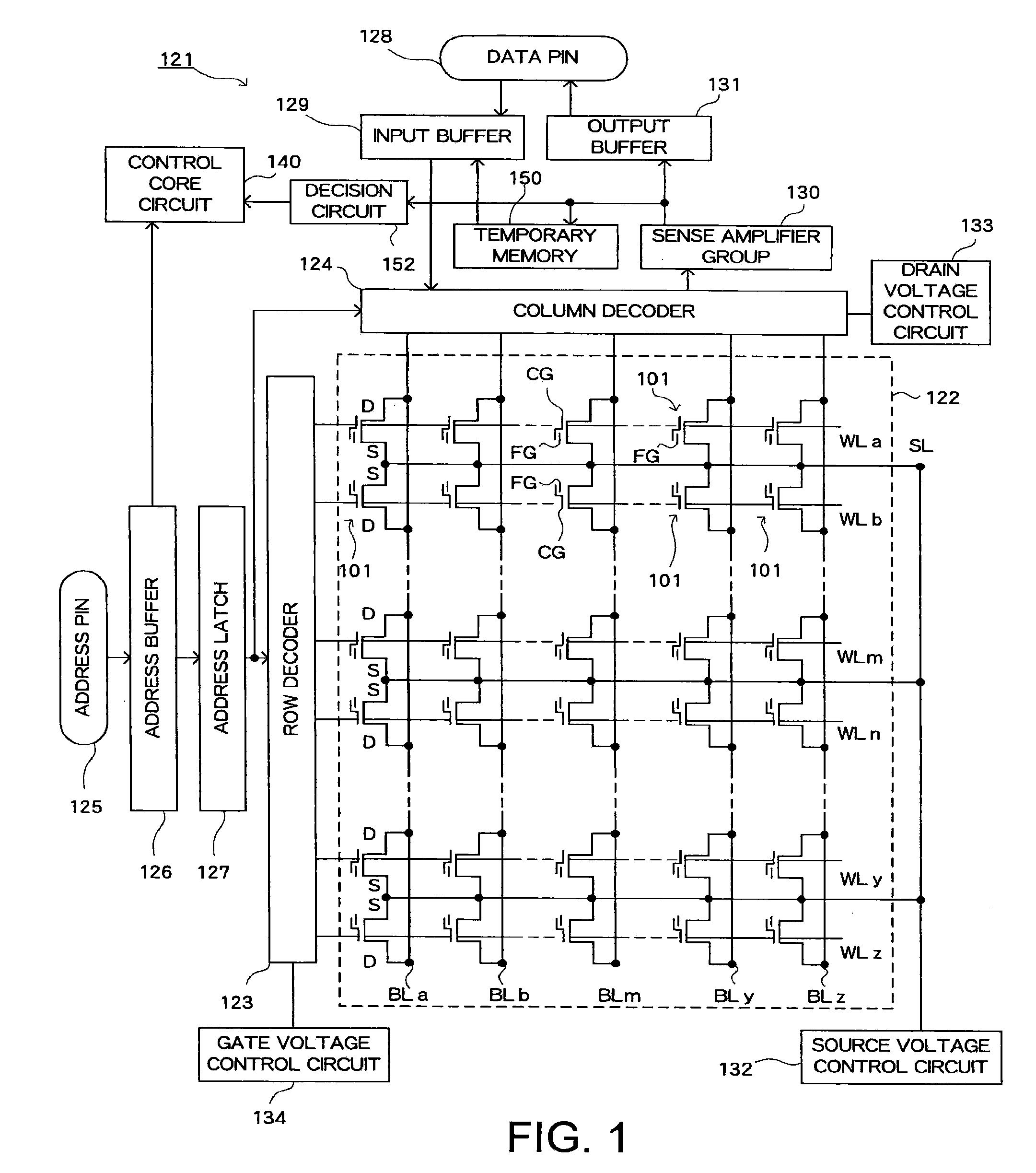
[0017]FIG. 1 shows an overall configuration of a flash EEPROM 121. Each memory cell 101 utilizes a split gate non-volatile semiconductor memory cell 101 including a source S, a channel CH, a drain D, a floating gate FG, and a control gate CG formed on a semiconductor substrate.

[0018]A sector 122, which is one set of unit memory cells, is composed of a plurality of memory cells 101 arranged in a matrix configuration. To control gates CG of memory cells 101 arranged in rows are respectively connected common word lines WLa to WLz. To drains D of memory cells 101 arranged in columns are respectively connected common bit lines BLa to BLz. Sources S of all memory cells 101 are connected to a common source line SL.

[0019]Word lines WLa to WLz are connected to a row decoder 123 and bit lines BLa to BLz are connected to a column decoder 124.

[0020]A row address and a column address ...


PUM


Abstract

An efficient erasure is performed. The voltage of a source line SL is manipulated in units of a sector comprising a plurality of memory cells. An erase command is received for the desired memory cells to be erased in a plurality of word line WL units arranged within a sector and all data within the sector, which includes the desired memory cells to be erased, is saved in a separate memory. Erasure is then performed for the entire sector, and among the saved data the data outside the desired memory cells to be erased is returned to the memory cells.

Description

CROSS-REFERENCE TO RELATED APPLICATION[0001]The entire disclosure of Japanese Patent Application No. 2008-148844 including specification, claims, drawings and abstract is incorporated herein by reference in its entirety.BACKGROUND OF THE INVENTION[0002]1. Field of the Invention[0003]The present invention relates to a non-volatile memory control circuit for controlling erasure of non-volatile memory where source line voltage is manipulated in units of a sector composed of a predetermined plurality of memory cells.[0004]2. Description of the Related Art[0005]Heretofore, flash memory has become widely popular as non-volatile memory to which data can be rewritten. Data erasure in flash memory is accomplished by applying a high voltage HV to a word line (WL) and removing electrons held in a floating gate (FG) of the memory.[0006]On the other hand, in a programming operation for writing data, a high voltage is applied to the source line. Since the high voltage is also applied to memory ce...

Claims


Application Information

Patent Timeline
Patent Type & Authority Applications(United States)
IPC IPC(8): G11C11/34G11C16/04
CPCG11C8/06G11C8/08G11C16/3431G11C16/16G11C16/3418G11C8/10
Inventor KANEDA, YOSHINOBU
Owner SEMICON COMPONENTS IND LLC
Why Eureka
Try Eureka