Thin film transistor, semiconductor device and electronic device

Active Publication Date: 2009-12-31
SEMICON ENERGY LAB CO LTD
View PDF101 Cites 32 Cited by
  • Summary
  • Abstract
  • Description
  • Claims
  • Application Information

AI Technical Summary

Benefits of technology

[0024]According to the present invention, as compared to a thin film transistor in which an amorphous semiconductor is included in a channel formation region, on-current of a thin film transistor can b

Problems solved by technology

A thin film transistor in which a channel is formed using an amorphous silicon layer has problems such as low field-effect mobility and low on-current.
On the other hand, a thin film transistor in which a channel is formed using a microcrystalline silicon layer has a problem in that, whereas the field-effect mobility is higher than that of the thin film transistor in which a channel is formed using an amorphous silicon layer, the off-current is high, and thus sufficient switching characteristics cannot be obt

Method used


Image

  • Thin film transistor, semiconductor device and electronic device
  • Thin film transistor, semiconductor device and electronic device
  • Thin film transistor, semiconductor device and electronic device

Examples


Example

Embodiment 1

[0056]In this embodiment, an example of a mode of a thin film transistor will be described with reference to the drawings.

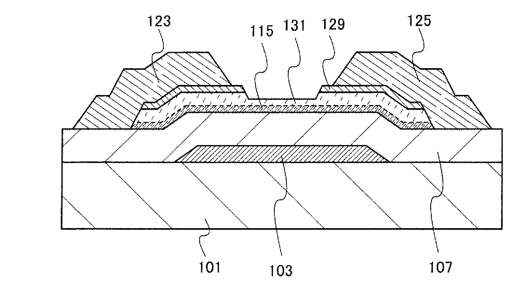
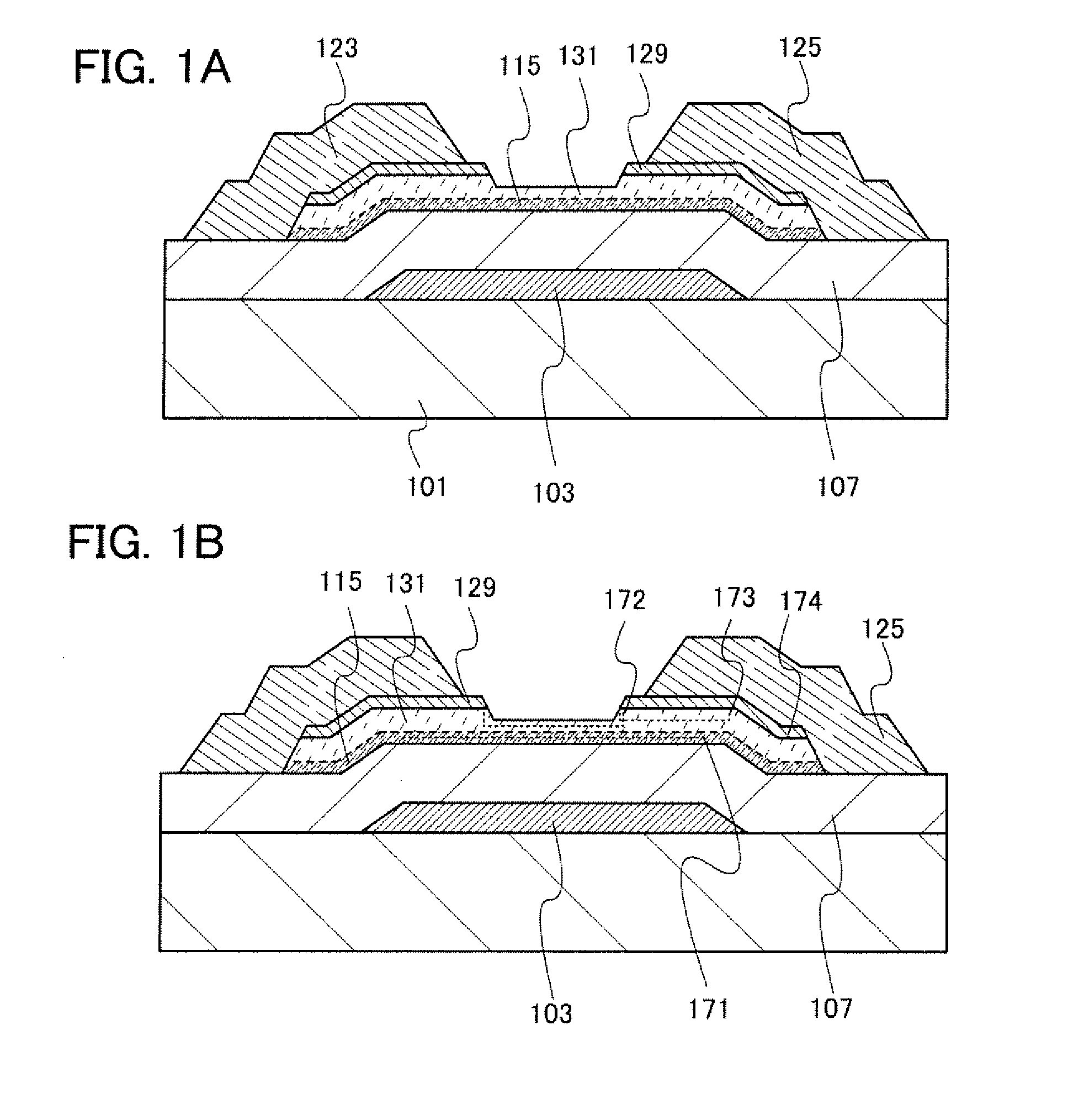
[0057]FIGS. 1A and 1B are cross-sectional views of a thin film transistor according to this embodiment. A thin film transistor illustrated in FIG. 1A includes a gate electrode layer 103 over a substrate 101; a gate insulating layer 107 which covers the gate electrode layer 103; a semiconductor layer 115 which is provided over and in contact with the gate insulating layer 107 and serves as a channel formation region; a buffer layer 131 over the semiconductor layer 115; and source and drain regions 129 which are in contact with part of the buffer layer 131. In addition, the thin film transistor includes a wiring layer 123 and a wiring layer 125 which are provided over and in contact with the source and drain regions 129. The wiring layer 123 and the wiring layer 125 form a source electrode and a drain electrode. Further, each layer has been patterned in...

Example

Embodiment 2

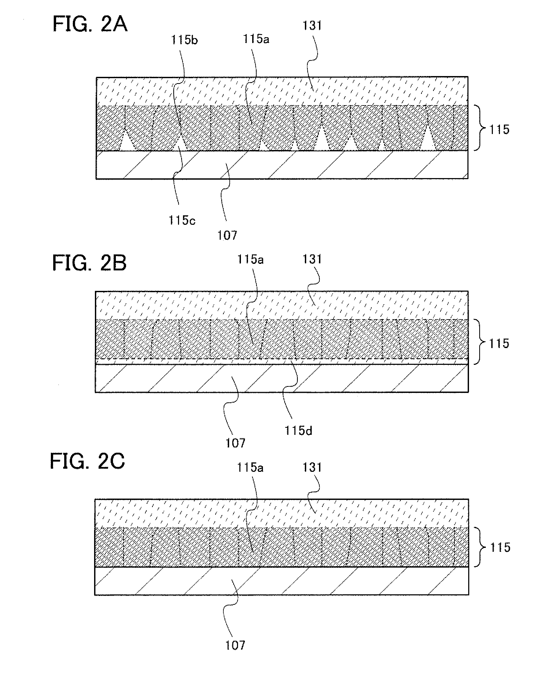
[0091]In this embodiment, modes which can be used for the semiconductor layer 115 in the thin film transistor described in Embodiment 1 will be described with reference to FIGS. 7A and 7B and FIGS. 8A and 8B. FIG. 7A is a cross-sectional view of a thin film transistor and FIG. 7B is an enlarged view of a region in which the gate insulating layer 107, a microcrystalline semiconductor 118, and the buffer layer 131 are in contact with each other.

[0092]As illustrated in FIGS. 7A and 7B, in a thin film transistor described in this embodiment, dispersed microcrystalline semiconductor particles or a net-like microcrystalline semiconductor 118 are formed over the gate insulating layer 107.

[0093]Dispersed microcrystalline semiconductor particles 118a can be formed using silicon, silicon germanium (SixGe1-x, 0.513 / cm3, preferably less than 1×10¹⁰ / cm3, the dispersed microcrystalline semiconductor particles can be formed by only deposition.

[0094]The diameter of the dispersed microcr...

Example

Embodiment 3

[0099]In this embodiment, a mode of a thin film transistor which is different from that described in Embodiment 1 will be described with reference to FIGS. 9A and 9B.

[0100]FIG. 9A is a cross-sectional view taken along a line A-B of FIG. 9B illustrating a thin film transistor of this embodiment. A thin film transistor illustrated in FIG. 9A includes a gate electrode layer 103 over a substrate 101; a gate insulating layer 107 which covers the gate electrode layer 103; a semiconductor layer 143 which is provided over and in contact with the gate insulating layer 107 and serves as a channel formation region; a buffer layer 159 over the semiconductor layer 143; and source and drain regions 157 which are in contact with part of the buffer layer 159. In addition, the thin film transistor includes a wiring layer 153 and a wiring layer 155 which are provided over and in contact with the source and drain regions 157. The wiring layer 153 and the wiring layer 155 form a source elec...


PUM


Abstract

A thin film transistor includes, as a buffer layer, an amorphous semiconductor layer having nitrogen or an NH group between a gate insulating layer and source and drain regions and at least on the source and drain regions side. As compared to a thin film transistor in which an amorphous semiconductor is included in a channel formation region, on-current of a thin film transistor can be increased. In addition, as compared to a thin film transistor in which a microcrystalline semiconductor is included in a channel formation region, off-current of a thin film transistor can be reduced.

Description

TECHNICAL FIELD[0001]The present invention relates to a thin film transistor and a method for manufacturing the thin film transistor, and a semiconductor device and a display device using the thin film transistor.BACKGROUND ART[0002]As a kind of field-effect transistor, a thin-film transistor in which a channel region is formed in a semiconductor layer formed over a substrate having an insulating surface is known. Techniques in which amorphous silicon, microcrystalline silicon, or polycrystalline silicon is used for the semiconductor layer used in the thin-film transistor have been disclosed (see Patent Documents 1 to 5). A typical application of a thin-film transistor is a liquid crystal television device, and the thin film transistor has been put to the practical use as a switching transistor for each pixel included in a display screen.REFERENCE[Patent Document][0003][Patent Document 1] Japanese Published Patent Application No. 2001-053283[0004][Patent Document 2] Japanese Publish...

Claims


Application Information

Patent Timeline
IPC IPC(8): H01L29/786H05B44/00
CPCH01L27/1214H01L29/04H01L27/1288H01L29/78696H01L29/66765H01L29/458
Inventor ISA, TOSHIYUKIJINBO, YASUHIROTEZUKA, SACHIAKIDAIRIKI, KOJIMIYAIRI, HIDEKAZUYAMAZAKI, SHUNPEI
Owner SEMICON ENERGY LAB CO LTD
Why Eureka
Try Eureka