Liquid crystal display panel and manufacturing method thereof
a liquid crystal display panel and liquid crystal technology, applied in static indicating devices, non-linear optics, instruments, etc., can solve the problems of disorientation, light leakage, and difficulty in controlling the arrangement of liquid crystal molecules in certain areas, so as to improve light leakage and non-uniform display
- Summary
- Abstract
- Description
- Claims
- Application Information
AI Technical Summary
Benefits of technology
Problems solved by technology
Method used
Image
Examples
first embodiment
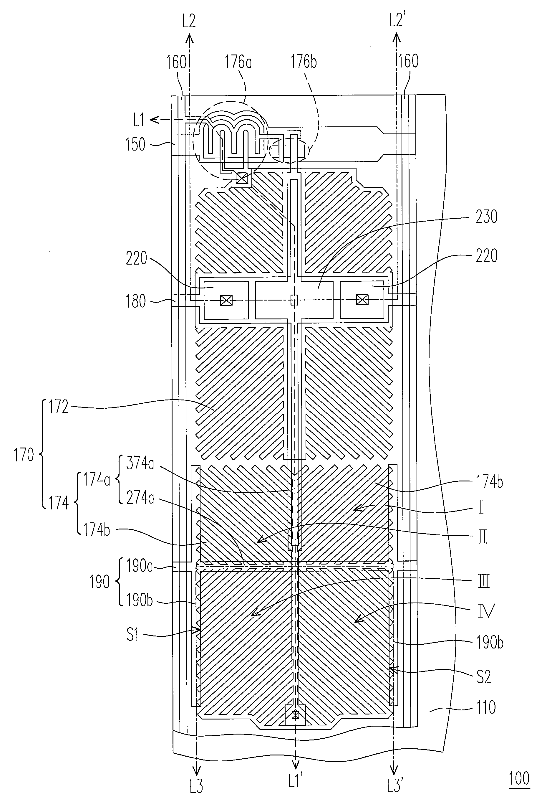
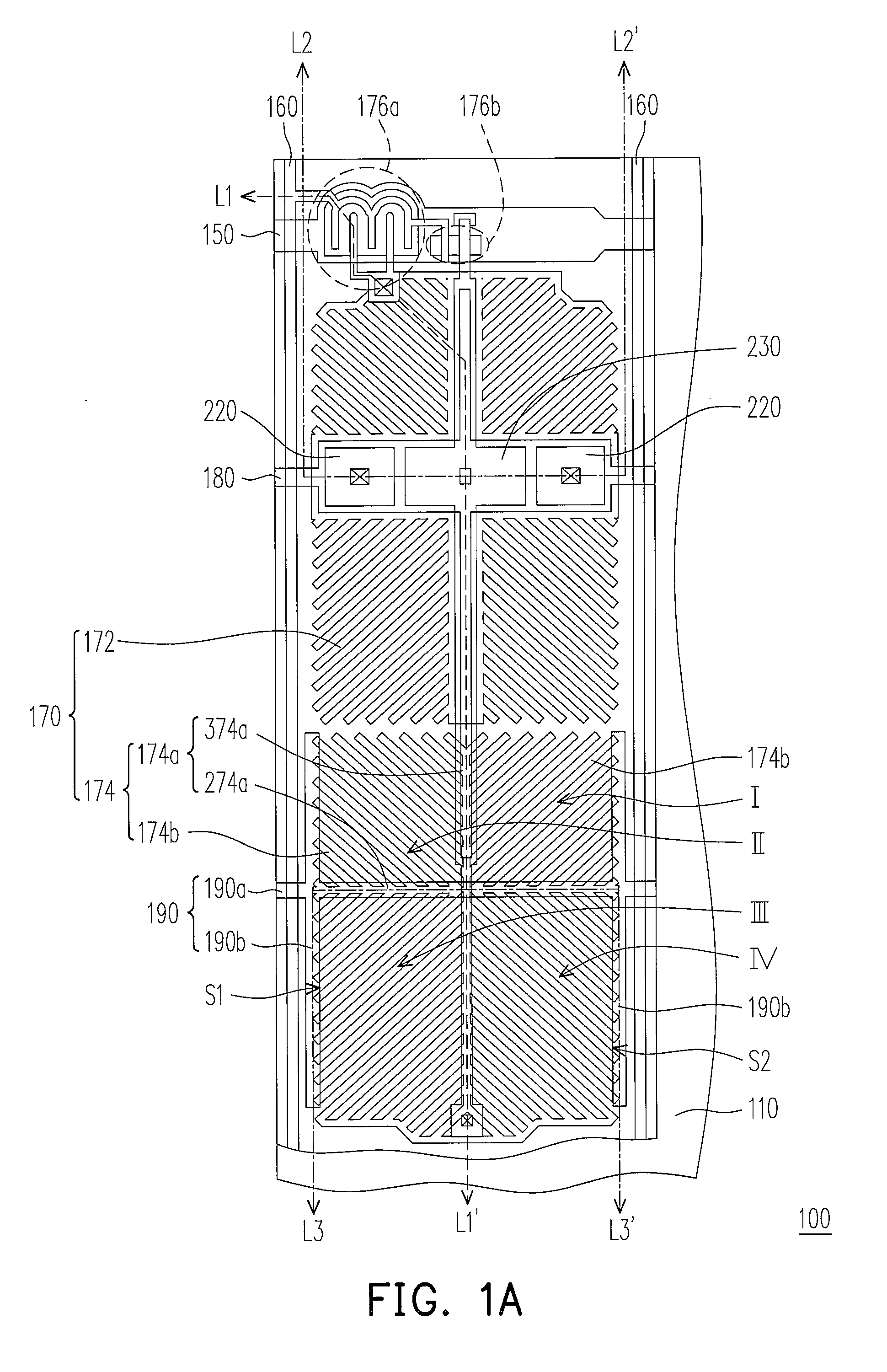
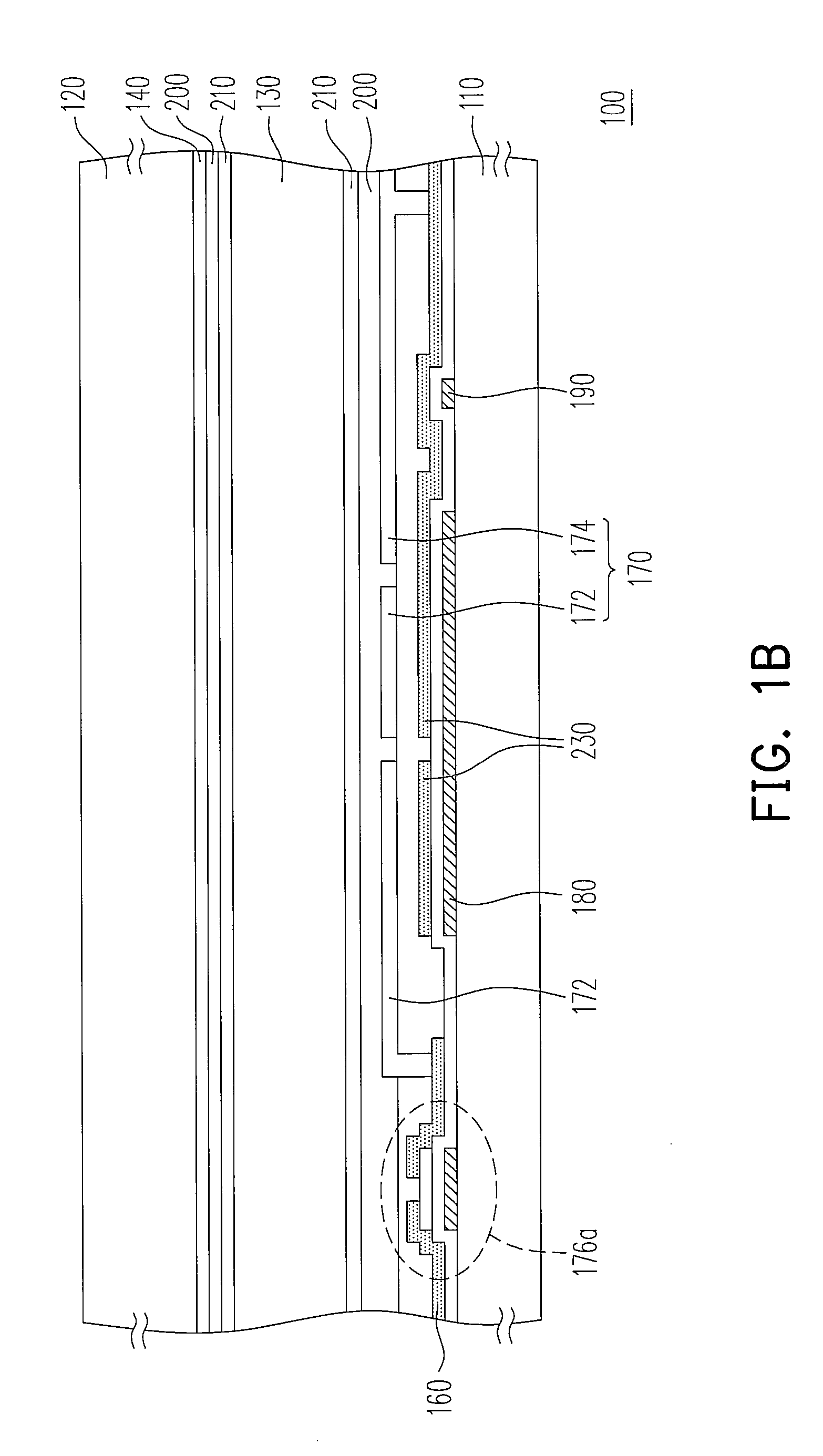
[0048]FIG. 1A illustrates a schematic view of a liquid crystal display panel according to the first embodiment of the present invention, and FIG. 1B illustrates a cross-sectional view along Line L1-L1′ in FIG. 1A. Referring to FIGS. 1A and 1B, a liquid crystal display panel 100 comprises a first substrate 110, a second substrate 120, a liquid crystal layer 130, an opposing electrode 140, a plurality of scan lines 150, a plurality of data lines 160, a plurality of pixel structures 170, a plurality of first capacitor bottom electrodes 180, a plurality of second capacitor bottom electrodes 190, at least an alignment layer 200, and at least a polymer layer 210. The liquid crystal display panel 100 is substantially a polymer stabilized alignment liquid crystal display panel. Herein, FIGS. 1A and 1B merely illustrate a part of the elements in an area of one pixel structure 170.
[0049]Based on the above, the second substrate 120 is opposite to the first substrate 110, and the liquid crystal...
second embodiment
[0073]FIG. 2 illustrates a partial top view of a liquid crystal display panel according to the second embodiment of the present invention, and FIG. 2 only illustrates the area of one pixel structure. Referring to FIG. 2, a liquid crystal display panel 400 in this embodiment is similar to the liquid crystal display panel 100 described in the first embodiment. It is to say that FIG. 2 which illustrates this embodiment is similar to FIG. 1A which illustrates the first embodiment, wherein the same elements are indicated by the same reference numbers. The descriptions thereof are therefore not repeated here.
[0074]As shown in FIG. 2, in this embodiment, a V-shaped main slit MS is formed between a first pixel electrode 472 and a second pixel electrode 474 of a pixel structure 470, wherein the V-shaped main slit MS comprises a pointed end MS1 and two side sections MS2 connected to the pointed end MS1. The pointed end MS1 is pointed toward the second pixel electrode 474, and an edge E1 of th...
third embodiment
A Third Embodiment
[0080]FIG. 3A illustrates a partial top view of a liquid crystal display panel according to the third embodiment of the present invention, and FIG. 3A only illustrates the area of one pixel structure. A liquid crystal display panel 700 in this embodiment is similar to the liquid crystal display panel 100 described in the first embodiment. It is to say that FIG. 3A which illustrates this embodiment is similar to FIG. 1A which illustrates the first embodiment, wherein the same or similar elements are indicated by the same or similar reference numbers. The descriptions thereof are therefore not repeated here.
[0081]Referring to FIG. 3A, the liquid crystal display panel 700 in this embodiment comprises a plurality of data lines 760, a plurality of pixel structures 770, a plurality of first capacitor bottom electrodes 780, and a plurality of second capacitor bottom electrodes 190 which are substantially different from those described in the first embodiment.
[0082]As show...
PUM
 Abstract
Description
Claims
Application Information


