Method for improving assembling deviation of liquid crystal display panel and manufacturing technology of liquid crystal panel

A technology of liquid crystal display panel and manufacturing process, which is applied in the direction of photolithographic exposure device, semiconductor/solid-state device manufacturing, static indicator, etc., can solve the problems such as light leakage, and achieve the advantages of not easy light leakage, improved assembly deviation, and good display quality Effect

Inactive Publication Date: 2006-04-12
CHUNGHWA PICTURE TUBES LTD
View PDF0 Cites 14 Cited by
  • Summary
  • Abstract
  • Description
  • Claims
  • Application Information

AI Technical Summary

Problems solved by technology

[0005] In view of this, the object of the present invention is to provide a method for improvin

Method used


Image

  • Method for improving assembling deviation of liquid crystal display panel and manufacturing technology of liquid crystal panel
  • Method for improving assembling deviation of liquid crystal display panel and manufacturing technology of liquid crystal panel
  • Method for improving assembling deviation of liquid crystal display panel and manufacturing technology of liquid crystal panel

Examples


Embodiment Construction

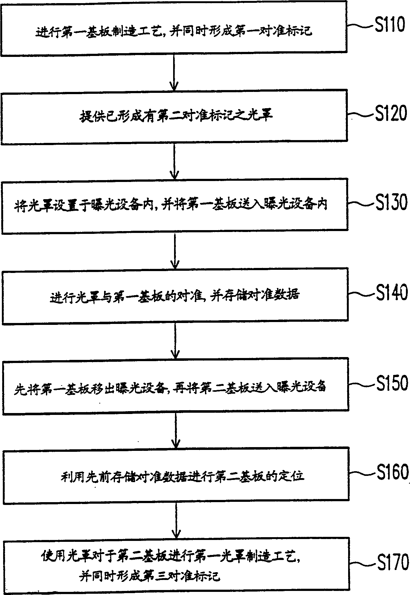
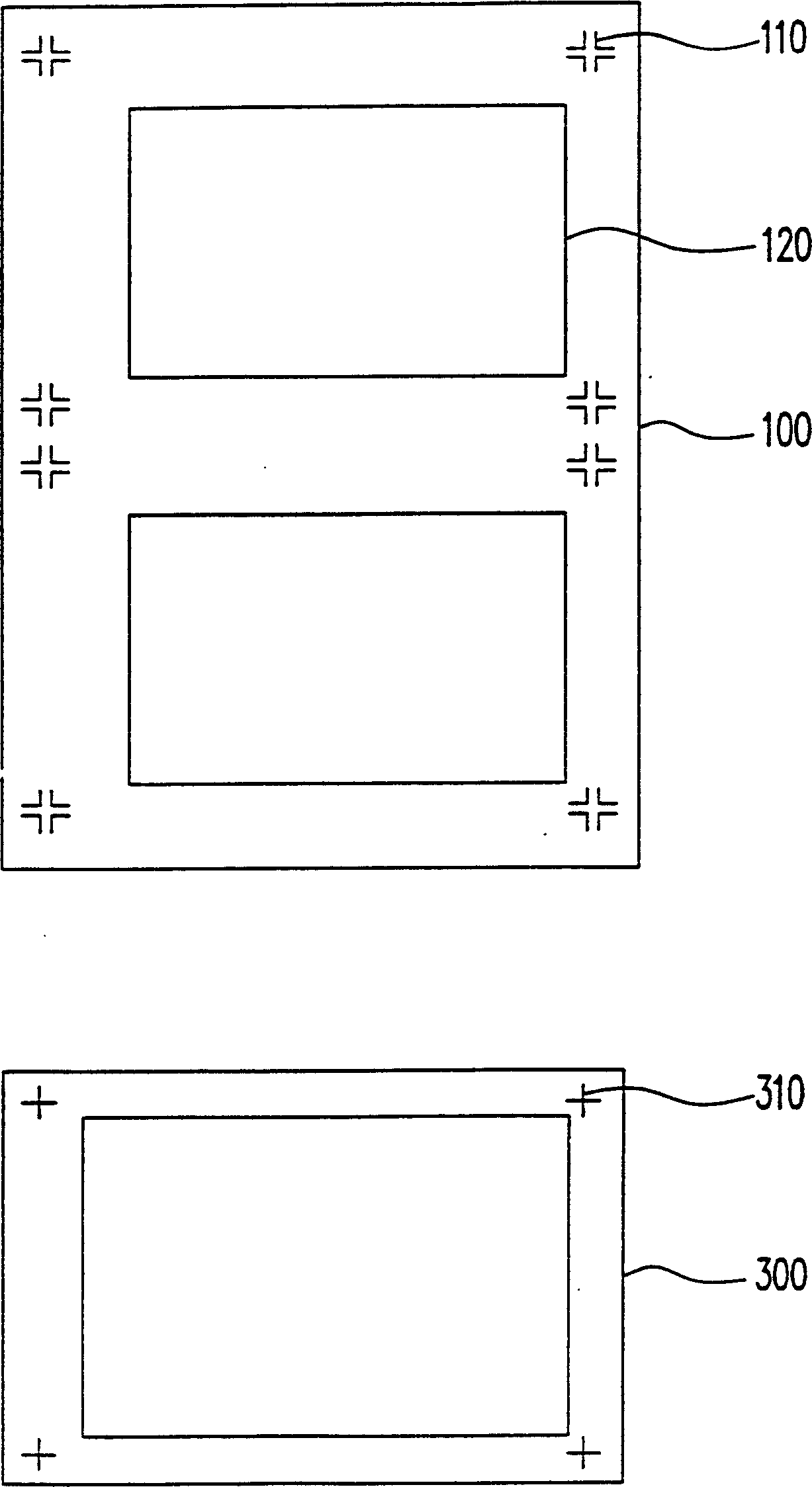
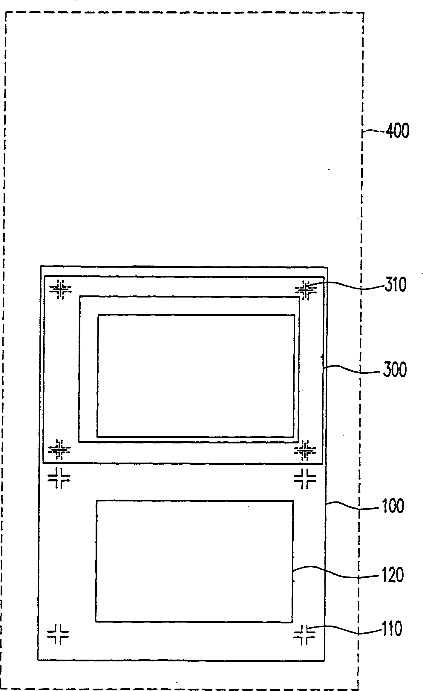
[0019] figure 1 A flow chart showing a method for improving assembly deviation of a liquid crystal display panel according to a preferred embodiment of the present invention, and Figure 2A to Figure 2F A schematic diagram showing a manufacturing process of a liquid crystal display panel according to a preferred embodiment of the present invention. Please refer to figure 1 and Figure 2A , firstly, step S110 is to perform a process step on the first substrate 100 and simultaneously form the first alignment mark 110 on the first substrate 100 . In particular, in the step of performing a process step on the first substrate 100, for example, a plurality of first pattern regions 120 are formed on the first substrate 100, and the first alignment mark 110 is formed on each first pattern region 120, for example. In the corner, the present invention does not limit the quantity and arrangement of the first pattern area 120 and the first alignment mark 110 , and the present invention...


PUM


Abstract

A method for improving the offset of the assembly of a LCD panel includes the following steps: forming a first aligning mark on the first base plate, providing a lampshade with a second aligning mark formed, designing the lampshade in an exposing device and sending the first base plate in it, aligning the two aligning marks on the lampshade and storing the aligning data, moving the first base plate out of the exposing device then moving the second in it, locating the second base plate by the data stored, manufacturing a first lampshade in terms of the lampshade and forming a third aligning mark corresponding to the second mark on the second base plate.

Description

technical field [0001] The present invention relates to a method for improving assembly shift and a manufacturing process of a display panel, and in particular relates to a method for improving assembly shift of a liquid crystal display panel and a manufacturing process of a liquid crystal display panel. Background technique [0002] Due to the increasing demand for displays, the industry is fully committed to the development of related displays. Among them, the cathode ray tube (Cathode Ray Tube) has been monopolizing the display market for many years due to its excellent display quality and technological maturity. However, due to the rise of the concept of green environmental protection, the characteristics of large energy consumption and large radiation, and the limited space for product flattening, it cannot meet the market demand for light, thin, short, small, beautiful and low power consumption. market trends. Therefore, thin film transistor liquid crystal displays (...

Claims


Application Information

Patent Timeline
IPC IPC(8): G02F1/136G02F1/133G03F7/20H01L21/00G02B5/23
Inventor 涂志中玉鸿典
Owner CHUNGHWA PICTURE TUBES LTD
Why Eureka
Try Eureka