Array substrate and touch display panel

An array substrate and substrate technology, applied in the field of array substrates and touch display panels, can solve the problems of signal attenuation, increase in thickness of touch traces 120, time increase, etc., and achieve the effect of alleviating color shift in color mixing

Active Publication Date: 2016-10-12
XIAMEN TIANMA MICRO ELECTRONICS +1
View PDF5 Cites 16 Cited by
  • Summary
  • Abstract
  • Description
  • Claims
  • Application Information

AI Technical Summary

Problems solved by technology

However, the increased thickness of the touch wiring 120 makes the upper surface of the touch wiring 120 protrude upwards, which intensifies the risk of light leakage on the display panel where the array substrate 100 is located.
In addition, when the thickness of the touch wiring 120 continues to increase, the time for the process of the touch wiring 120 (such as wet etching) increases, resulting in a decrease in the critical dimension of the touch wiring 120, resulting in a decrease in the cross-sectional area of ​​the touch wiring 120. decreases, which in turn leads to a relative increase in the resistance of the touch trace 120
It can be seen that this method will also cause signal attenuation, which will lead to poor display.

Method used


Image

  • Array substrate and touch display panel
  • Array substrate and touch display panel
  • Array substrate and touch display panel

Examples


no. 1 example

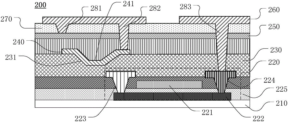
[0033] see first image 3 and Figure 4 , image 3 Showing a cross-sectional view of the array substrate 200 according to the first embodiment of the present invention, Figure 4 show image 3 A partial enlarged view of the array substrate 200 of FIG.

[0034] The array substrate 200 includes: a substrate 210 , a plurality of switch elements 220 , a first insulating layer 230 , a touch electrode layer and a touch wiring layer.

[0035] A plurality of switching elements 220 are located above the substrate 210 . The switching element 220 may be a thin film transistor. For example, in image 3 In the illustrated embodiment, the switch element 220 is a top-gate thin film transistor. Each top-gate TFT 220 includes an active layer 222 , a gate insulating layer 225 , a gate 221 , a source 223 , and a drain 224 sequentially on the substrate 210 . The source electrode 223 and the drain electrode 224 are located on the same layer. The switch element 220 can also be a bottom-gat...

no. 2 example

[0047] see Figure 5 , Figure 5 A cross-sectional view of an array substrate 300 according to a second embodiment of the present invention is shown. Figure 5 The structure of the array substrate 300 shown is the same as image 3 The illustrated array substrate 200 has a similar structure. and image 3 The difference of the array substrate 200 shown is that the concave portion 331 of the array substrate 300 is perpendicular to the cross-section of the extending direction of the touch trace 340 (eg Figure 5 The section shown) is V-shaped. The V-shaped concave portion 331 can not only alleviate the problem of light leakage, but also alleviate the problem of color shift in color mixing.

no. 3 example

[0049] see Figure 6 , Figure 6 A cross-sectional view of an array substrate according to a third embodiment of the present invention is shown. Figure 6 The structure of the array substrate 400 shown is the same as image 3 The illustrated array substrate 200 has a similar structure. and image 3 The difference of the array substrate 200 shown is that the fourth surface 443 of the convex part 441 of the touch trace 440 of the array substrate 400 away from the substrate 410 is not lower than the upper surface 432 of the first insulating layer 430 on the edge of the concave part (convex out of the third surface of portion 441 with image 3 The first surface 242 shown is the same, being in contact with the inner wall of the recess). M3 is made into a buried structure. Figure 6 In the illustrated embodiment, in addition to reducing the resistance of the touch wire 440 , it can also prevent the touch wire 440 from falling off on the first insulating layer 430 and reduce th...


PUM


Abstract

The invention provides an array substrate and a touch display panel comprising the array substrate. The array substrate comprises a substrate, multiple switch elements located above the substrate, a first insulation layer located above the switch elements and provided with an upper surface having at least one recess, a touch-control electrode layer located above the switch elements and provided with multiple touch-control electrodes, and a touch-control wiring layer located above the first insulation layer and provided with multiple touch-control wiring. Each touch-control wiring is electrically connected with each touch-control electrode correspondingly and used for connecting a corresponding touch-control electrode to a driving circuit. At least one touch-control wiring comprises at least one protrusion arranged in a corresponding recess. The array substrate and the touch display panel comprising the array substrate help improve display effect.

Description

technical field [0001] The present invention relates to the field of display technology, in particular to an array substrate and a touch display panel. Background technique [0002] With the development of human-computer interaction technology, touch technology is increasingly used on various displays. Capacitive touch technology is widely used due to its advantages of wear resistance, long life, low maintenance cost for users, and support for gesture recognition and multi-touch. [0003] Capacitive touch technology can be divided into self-capacitive touch technology and mutual-capacitive touch technology according to the detection method of capacitance between different objects. Self-capacitive touch technology detects the presence, position, and motion of an input object on a touch screen based on changes in capacitance between the input object and electrodes. The mutual capacitive touch technology detects the existence, position and movement of an input object on the t...

Claims


Application Information

Patent Timeline
Patent Type & Authority Applications(China)
IPC IPC(8): G06F3/044G06F3/041
CPCG06F3/0412G06F3/044G06F2203/04111G06F2203/04103
Inventor 文亮
Owner XIAMEN TIANMA MICRO ELECTRONICS
Why Eureka
Try Eureka