
Vapor deposition method and manufacturing device of vapor deposition thin film, vapor deposition thin film and display device8

An evaporation thin film and evaporation technology, which is applied in vacuum evaporation plating, sputtering plating, ion implantation plating, etc., can solve problems such as color mixing

Active Publication Date: 2018-12-18
BOE TECH GRP CO LTD +1
View PDF6 Cites 8 Cited by
  • Summary
  • Abstract
  • Description
  • Claims
  • Application Information

AI Technical Summary

Problems solved by technology

[0005] Embodiments of the present invention provide an evaporation method and production equipment for an evaporation film, an evaporation film, and a display device, which can solve the problem of color mixing between adjacent evaporation patterns in the prior art due to overlapping

Method used


Image

  • Vapor deposition method and manufacturing device of vapor deposition thin film, vapor deposition thin film and display device8
  • Vapor deposition method and manufacturing device of vapor deposition thin film, vapor deposition thin film and display device8
  • Vapor deposition method and manufacturing device of vapor deposition thin film, vapor deposition thin film and display device8

Examples


Embodiment 1

[0051] In the above, the relative distance between the first evaporation pattern 101 and the second evaporation pattern 102 is adjusted by modifying the original distance H1 between the first evaporation pattern 101 and the second evaporation pattern 102 in the evaporation unit of the original evaporation film. Locations include: (reference Figure 4 )

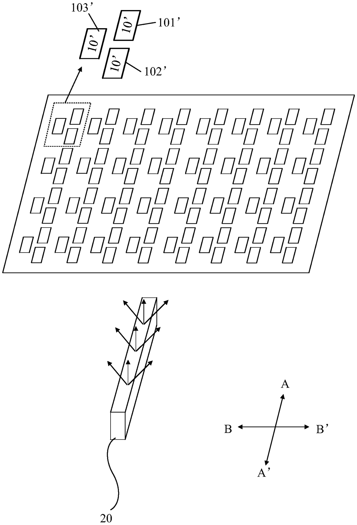
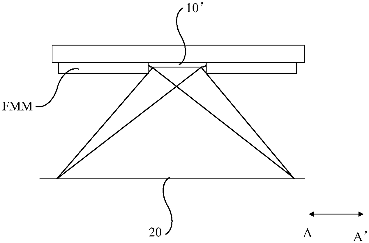
[0052] Step S101, refer to Figure 5 (a) of Figure 4 The schematic cross-sectional view of the first vapor deposition pattern 101' along the O1-O1' position in , measuring the mask shadow pattern of the vapor deposition pattern 10' in the original vapor deposition film along the first direction AA', one side A dimension (L1); Of course, the vapor deposition pattern 10' here can be Figure 2a Any one of the first vapor deposition pattern 101', the second vapor deposition pattern 102', and the third vapor deposition pattern 103' in the original vapor deposition film shown in Figure 4 The illustration is only schematically ...

Embodiment 2

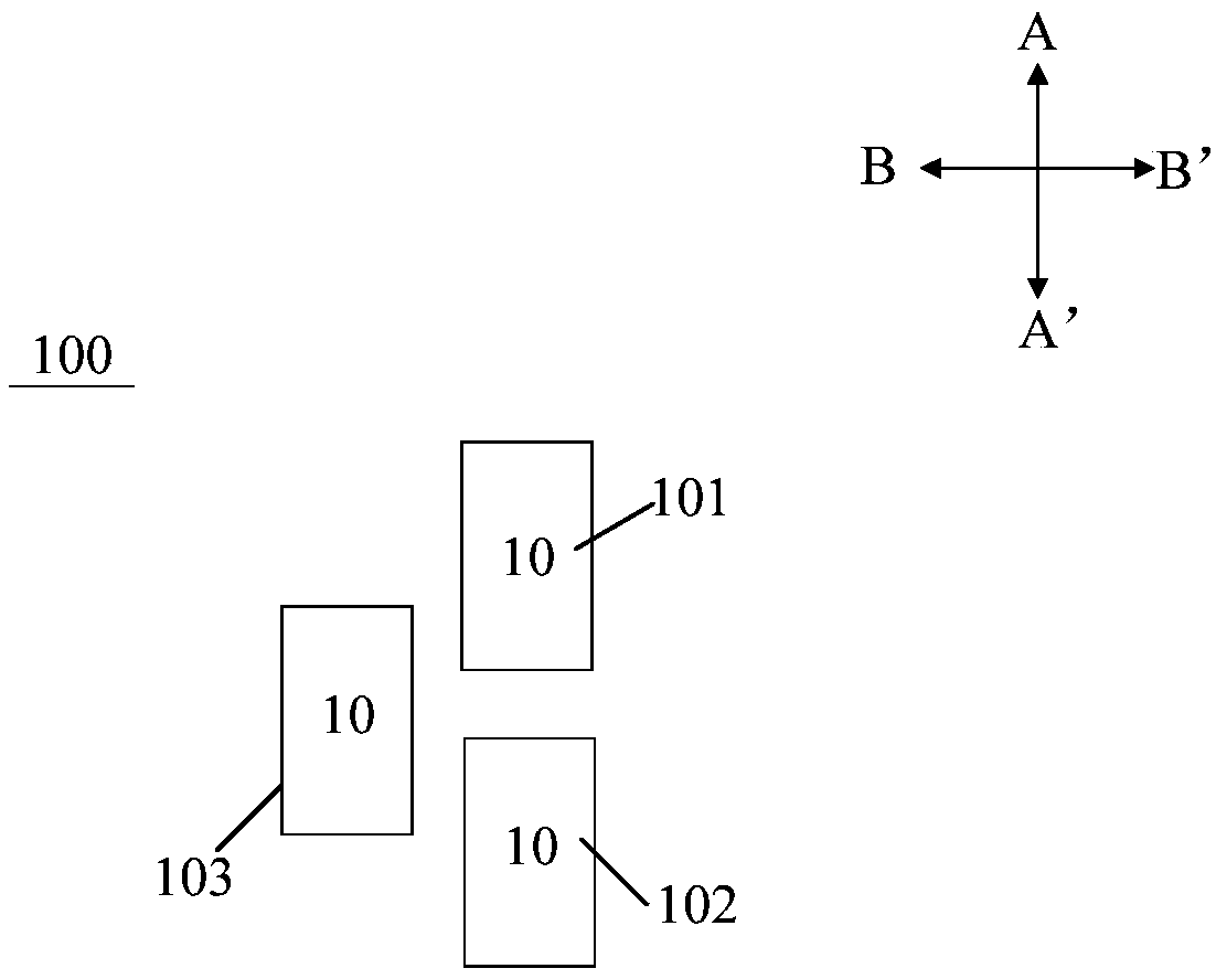
[0066] As can be seen from the foregoing, in practice, when using Figure 2a In the evaporated film formed by the evaporation method shown in , the mask shadow (Shadow) along the first direction A-A' will be significantly larger than the mask shadow along the second direction B-B' (refer to image 3 , Figure 4 , Figure 5 ), so that the risk of offset aliasing between the first vapor deposition pattern 101 and the second vapor deposition pattern 102 arranged side by side along the first direction A-A' is high, resulting in a high risk of color mixing.

[0067] Based on this, in this embodiment, the relative position of the first vapor deposition pattern 101 and the second vapor deposition pattern 102 is adjusted by adjusting the movement of the linear vapor deposition source 20 relative to the first vapor deposition pattern 101 and the second vapor deposition pattern 102 Including: (reference Figure 7 )

[0068] Using the first linear evaporation source 201 moving along ...

Embodiment 3

[0075] The aforementioned adjustment of the relative positions of the first vapor deposition pattern and the second vapor deposition pattern by adjusting the alignment method of the mask includes:

[0076] moving the first reticle along the first direction AA' and the second direction BB' (perpendicular to the first direction), and rotating the first reticle along the central axis of the first reticle, in the first reticle When the error of the distance from the stencil to the target position along the vertical first direction is within the standard error range, the error of the distance from the first mask to the target position along the first direction is minimized to form the first vapor deposition pattern 101 .

[0077] moving the second reticle along the first direction AA' and the second direction BB', and rotating the second reticle along the central axis of the second reticle, when the second reticle reaches the target position When the error of the distance along the...


PUM


Abstract

The embodiment of the invention provides a vapor deposition method and a manufacturing device of a vapor deposition thin film, the vapor deposition thin film and a display device, which relate to thetechnical field of display and can solve the problem of color mixing caused by overlapping between adjacent vapor deposition patterns in the prior art. The vapor deposition thin film to be formed in the vapor deposition method of the vapor deposition thin film comprises a plurality of vapor deposition units, each vapor deposition unit comprises a plurality of vapor deposition patterns, and the plurality of vapor deposition patterns comprise a first vapor deposition pattern and a second vapor deposition pattern arranged side by side in a first direction and adjacent to each other. The vapor deposition method comprises the following steps: by correcting the original spacing between the first vapor deposition pattern and the second vapor deposition pattern in the vapor deposition unit of theoriginal vapor deposition thin film, and / or adjusting the moving mode of a linear vapor deposition source relative to the first vapor deposition pattern and the second vapor deposition pattern, and / oradjusting the relative positions of the first vapor deposition pattern and the second vapor deposition pattern by adjustment of the alignment mode of a mask, the color mixing between two adjacent sub-pixels of different colors is reduced.

Description

technical field [0001] The invention relates to the field of display technology, in particular to an evaporation method and production equipment for an evaporation film, an evaporation film, and a display device. Background technique [0002] Organic Light Emitting Diode (OLED) displays have been widely used in computers, mobile phones, etc. Various electronic devices including electronic products. [0003] Wherein, during the actual manufacture of OLED display devices (especially AMOLED display devices), OLED materials are generally vapor-deposited on the substrate through a mask plate by vacuum evaporation to form patterns of various functional layers. [0004] However, in the evaporation process of OLED materials, the problem of evaporation shadow (Shadow) will inevitably occur, especially for linear evaporation sources, the shadow generated along the direction of linear evaporation source extension is more serious, As a result, disadvantages such as uneven thickness of...

Claims


Application Information

Patent Timeline
Patent Type & Authority Applications(China)
IPC IPC(8): C23C14/24C23C14/04H01L51/56
CPCC23C14/042C23C14/24H10K71/164
Inventor 张健黄俊杰王震曹飞
Owner BOE TECH GRP CO LTD
Learn More