

Method and system for step-and-align interference lithography
a technology of interference lithography and step-and-aligning, which is applied in the field of interference lithography (il) technology, can solve the problems of insufficient precision for manufacturing microstructures whose critical mobile platform of piezoelectric actuators is only capable of traveling in a very short stroke, and achieves high precision
- Summary
- Abstract
- Description
- Claims
- Application Information
AI Technical Summary
Benefits of technology
Problems solved by technology
Method used
Image

Examples
Embodiment Construction
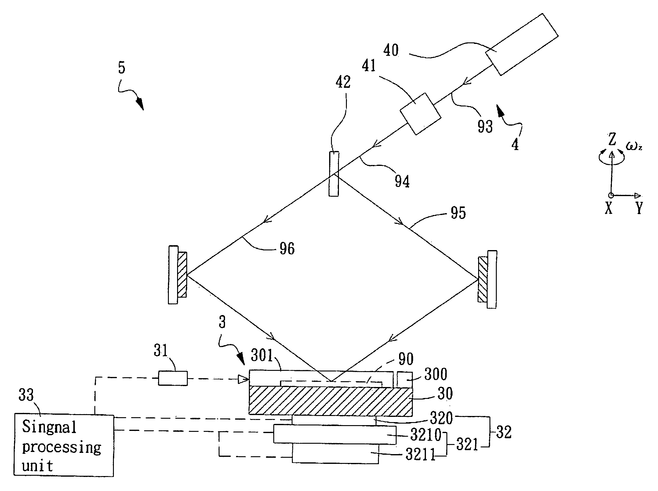
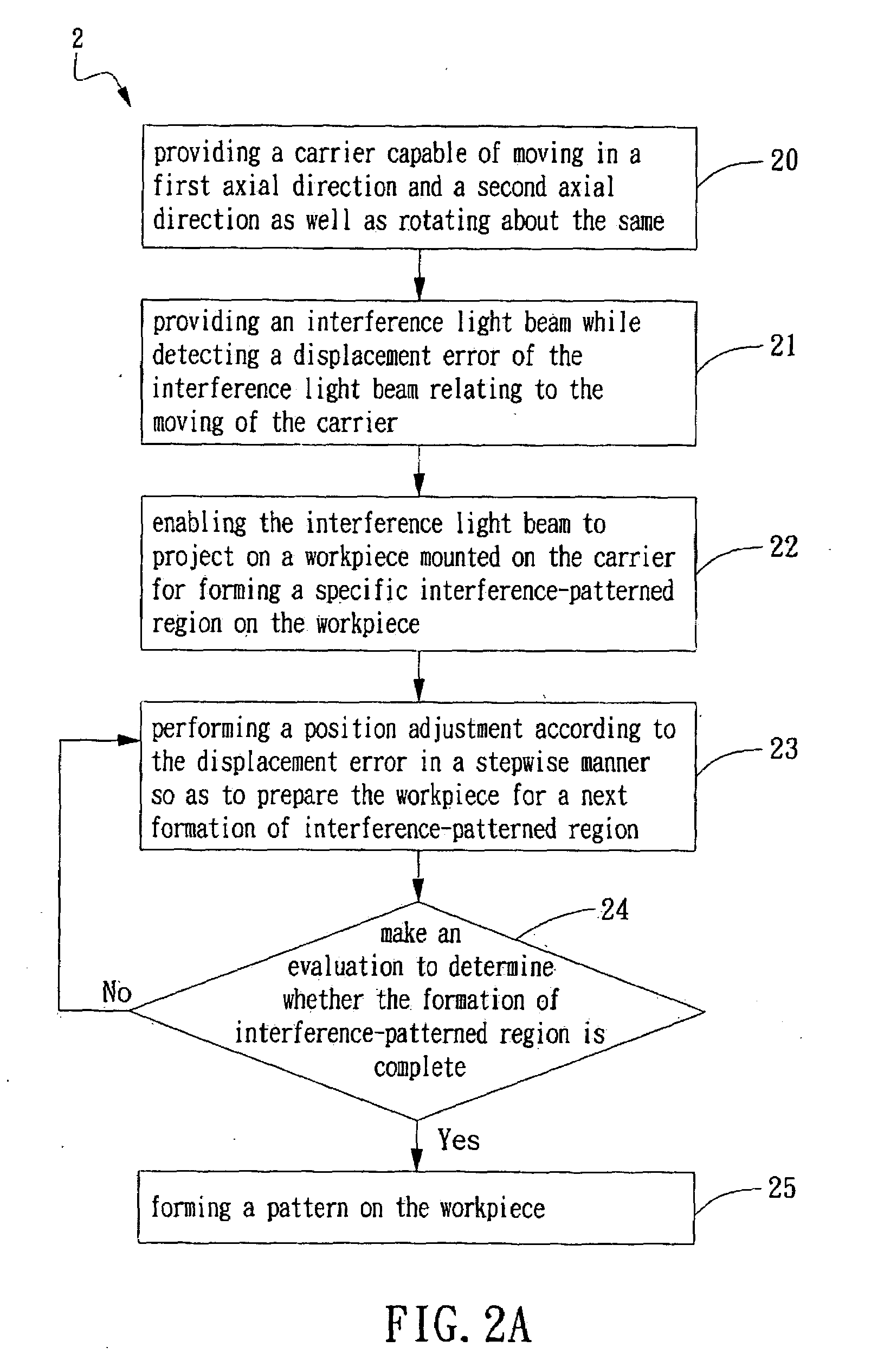
[0028]For your esteemed members of reviewing committee to further understand and recognize the fulfilled functions and structural characteristics of the invention, several exemplary embodiments cooperating with detailed description are presented as the follows. Please refer to FIG. 2A, which is a flow chart depicting the steps of a method for step-and-align interference lithography according to an exemplary embodiment of the invention. The method starts from step 20. At step 20, a carrier capable of moving in a first axial direction and a second axial direction as well as rotating about the same is provided, which is used for carrying a substrate for interference lithography whereas the substrate can be made of a silicon material, but is not limited thereby; and then the flow proceeds to step 21. At step 21, an interference light beam is provided and further g a displacement error of the interference light beam relating to the moving of the carrier is also being detected; and then t...
PUM
 Abstract
Description
Claims
Application Information