Bonded semiconductor structure and method of fabricating the same

a technology of bonded semiconductors and semiconductor materials, applied in the direction of semiconductor devices, basic electric elements, electrical appliances, etc., can solve the problems of reducing the processing efficiency of semiconductor materials, and forming horizontal and vertical semiconductor devices on a single major surface of a substrate. the temperature of the semiconductor material can be greater than 800, and the laser is capable of driving the temperature of the semiconductor material to be greater than 800

Inactive Publication Date: 2009-12-31
BESANG
View PDF62 Cites 234 Cited by
  • Summary
  • Abstract
  • Description
  • Claims
  • Application Information

AI Technical Summary

Problems solved by technology

However, these laterally oriented devices consume significant amounts of chip area.
However, forming both horizontal and vertical semiconductor devices on a single major surface of a substrate complicates the processing steps because the masks and processing steps needed are not compatible.
However, a disadvantage of this method is that the laser is capable of driving the temperature of the semiconductor material to be greater t...

Method used


Image

  • Bonded semiconductor structure and method of fabricating the same
  • Bonded semiconductor structure and method of fabricating the same
  • Bonded semiconductor structure and method of fabricating the same

Examples


Embodiment Construction

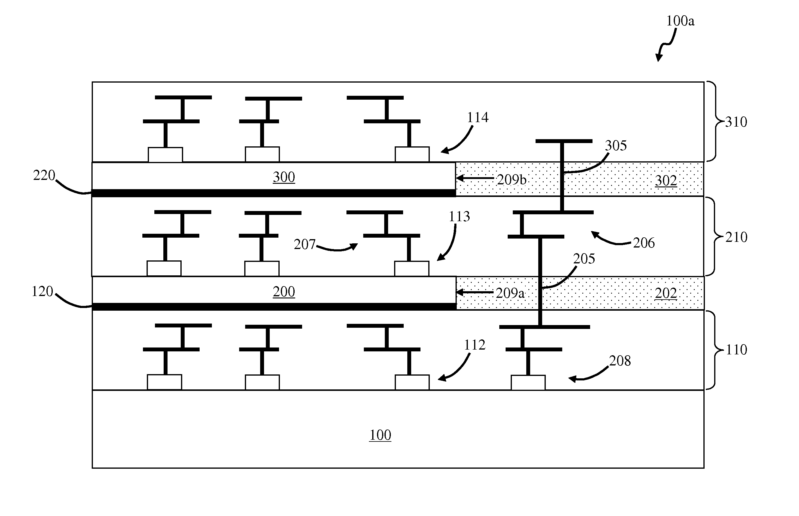
[0031]FIG. 1 is a cross-sectional view of one embodiment of a bonded semiconductor structure circuit 100a. Bonded semiconductor structure circuit 100a is a bonded semiconductor structure because, as discussed in more detail below, it includes a bonding region which bonds an electronic device to an interconnect region through a bonding interface. Other semiconductor structures are not bonded semiconductor structures because they do not include a bonding region which bonds an electronic device through a bonding interface.

[0032]In this embodiment, bonded semiconductor structure circuit 100a includes a support substrate 100 which carries an interconnect region 110 and a horizontally oriented semiconductor device 112. Horizontally oriented semiconductor device 112 is embodies as a single semiconductor device. However, it should be noted that a number of horizontally oriented semiconductor devices can be carried by support substrate 100, wherein the devices are connected together to opera...


PUM


Abstract

A method of forming a bonded semiconductor structure circuit includes providing a support substrate which carries a first semiconductor circuit and providing a first interconnect region carried by the support substrate. The method includes providing a bonded semiconductor substrate which is bonded to the first interconnect region through a bonding interface and forming a second semiconductor circuit which is carried by the first bonded semiconductor substrate.

Description

CROSS-REFERENCE TO RELATED APPLICATIONS[0001]This application claims the benefit of Korean Patent Application No. 10-2008-50946, filed on May 30, 2008, the contents of which are incorporated herein by reference.[0002]This application is a continuation-in-part of, and claims the benefit of, U.S. patent application Ser. No. 12 / 470,344, which claims the benefit of Republic of Korea Patent Application No. 10-2008-0046991, the contents of which are incorporated herein by reference.[0003]This application is a continuation-in-part of, and claims the benefit of, U.S. patent application Nos.:[0004]12 / 040,642, filed on Feb. 29, 2008,[0005]11 / 092,498, filed on Mar. 29, 2005, now U.S. Pat. No. 7,470,142,[0006]11 / 092,499, filed on Mar. 29, 2005, now U.S. Pat. No. 7,470,598,[0007]11 / 092,500, filed on Mar. 29, 2005,[0008]11 / 092,501, filed on Mar. 29, 2005;[0009]11 / 092,521, filed on Mar. 29, 2005;[0010]11 / 180,286, filed on Jul. 12, 2005;[0011]11 / 378,059, filed on Mar. 17, 2006; and[0012]11 / 606,523,...

Claims


Application Information

Patent Timeline
IPC IPC(8): H01L21/60H01L21/762
CPCH01L21/2007H01L21/8221H01L2924/1305H01L2924/1306H01L2924/0665H01L2924/01033H01L2924/01006H01L2224/2919H01L24/29H01L2924/19043H01L2924/19042H01L2924/19041H01L24/83H01L27/0688H01L2224/291H01L2224/8385H01L2924/01005H01L2924/01013H01L2924/01015H01L2924/01029H01L2924/01032H01L2924/0104H01L2924/01042H01L2924/0105H01L2924/01073H01L2924/01074H01L2924/04941H01L2924/04953H01L2924/07802H01L2924/13091H01L2924/14H01L2924/00H01L2924/3512
Inventor LEE, SANG-YUN
Owner BESANG
Why Eureka
Try Eureka