Flash memory device reducing noise of common source line, program verify method thereof, and memory system including the same

a flash memory and source line technology, applied in static storage, digital storage, instruments, etc., can solve problems such as reducing reliability, and achieve the effects of reducing noise, reducing noise, and reducing nois

Active Publication Date: 2010-01-07
SAMSUNG ELECTRONICS CO LTD
View PDF6 Cites 28 Cited by
  • Summary
  • Abstract
  • Description
  • Claims
  • Application Information

AI Technical Summary

Benefits of technology

[0011]Exemplary embodiments of the present invention are related to a flash memory device reducing noise in common source line, program verify method thereof, and memory system including the same. In an exemplary embodiment, a flash memory device may include a plurality of memory cells connected between a bit line and a common source line and a data input/output circuit connected to the bit line. The data input/output circuit is configured to store data to be programmed in a selected memory cell among the plurality of memory cells. The data input/output circuit is configured to maintain the data to be programmed during a program verify operation, and to decrease noise in the common source line by selectively precharging the bit lines based on the data to be programmed.
[0012]According to an exemplary embodiment, a program verify method of a flash memory device may include a plurality of memory cells connected between a bit line and a common source line, and a data input/output circuit connected to the bit line. The program verify method includes storing data to be programmed in a selected memory cel

Problems solved by technology

Noise generated in the common source line CSL may cause the threshold voltage distribution width of each state to be

Method used


Image

  • Flash memory device reducing noise of common source line, program verify method thereof, and memory system including the same
  • Flash memory device reducing noise of common source line, program verify method thereof, and memory system including the same
  • Flash memory device reducing noise of common source line, program verify method thereof, and memory system including the same

Examples


Embodiment Construction

[0026]Exemplary embodiments of the present invention will now be described more fully hereinafter with reference to the accompanying drawings. This invention, however, may be embodied in many different forms and should not be construed as limited to the embodiments set forth herein. In the drawings, the thicknesses of layers and regions may be exaggerated for clarity. Like numbers may refer to like elements throughout the accompanying figures.

[0027]Exemplary embodiments of the present invention may provide for a flash memory device capable of reducing or eliminating widening of threshold voltage distribution due to noise in a common source line.

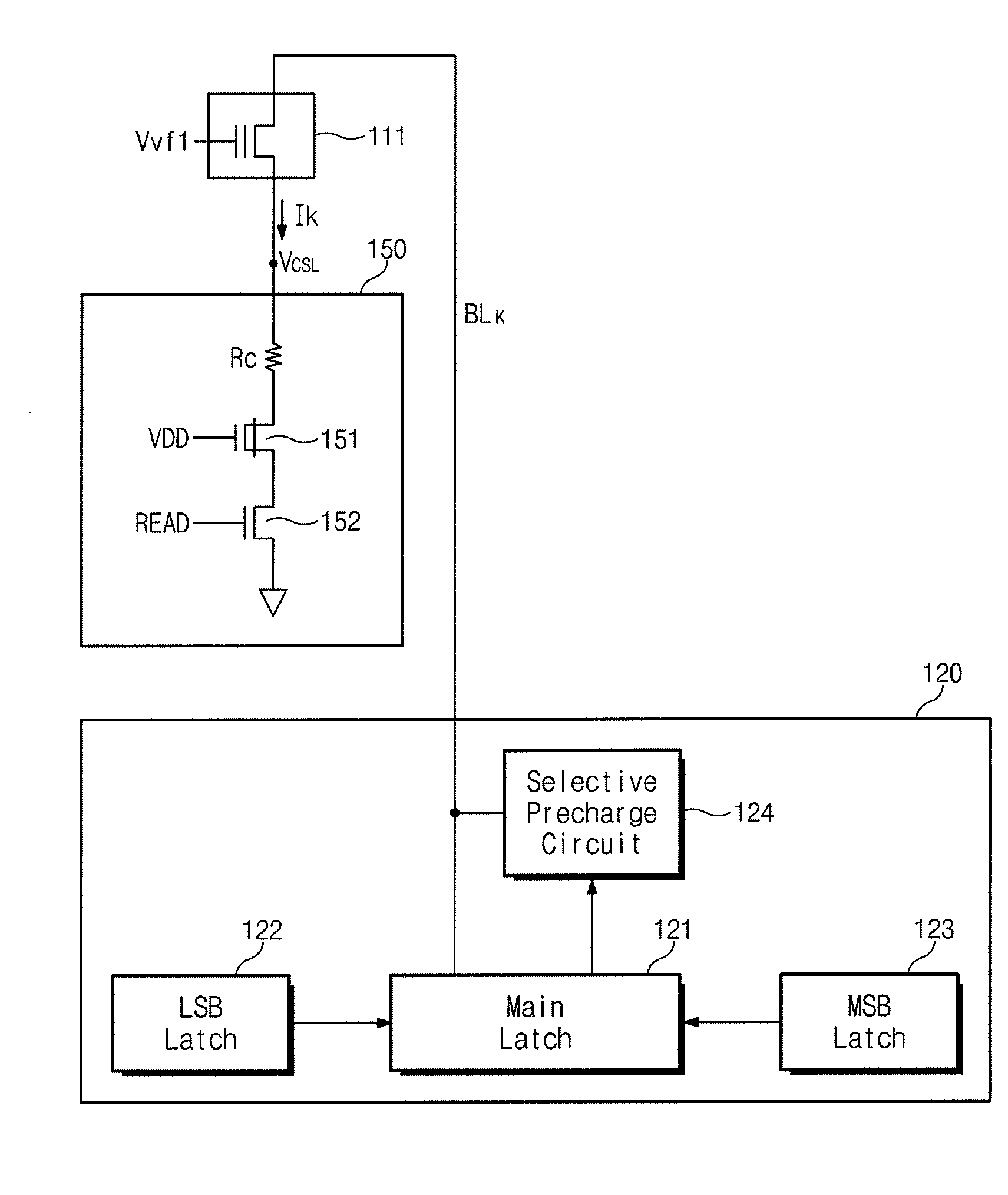
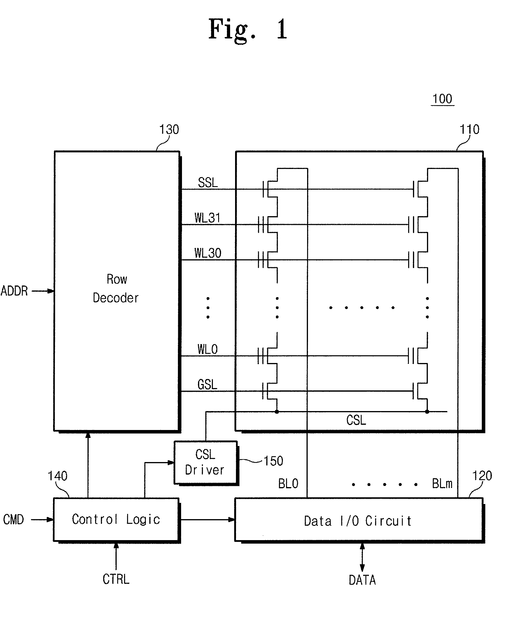
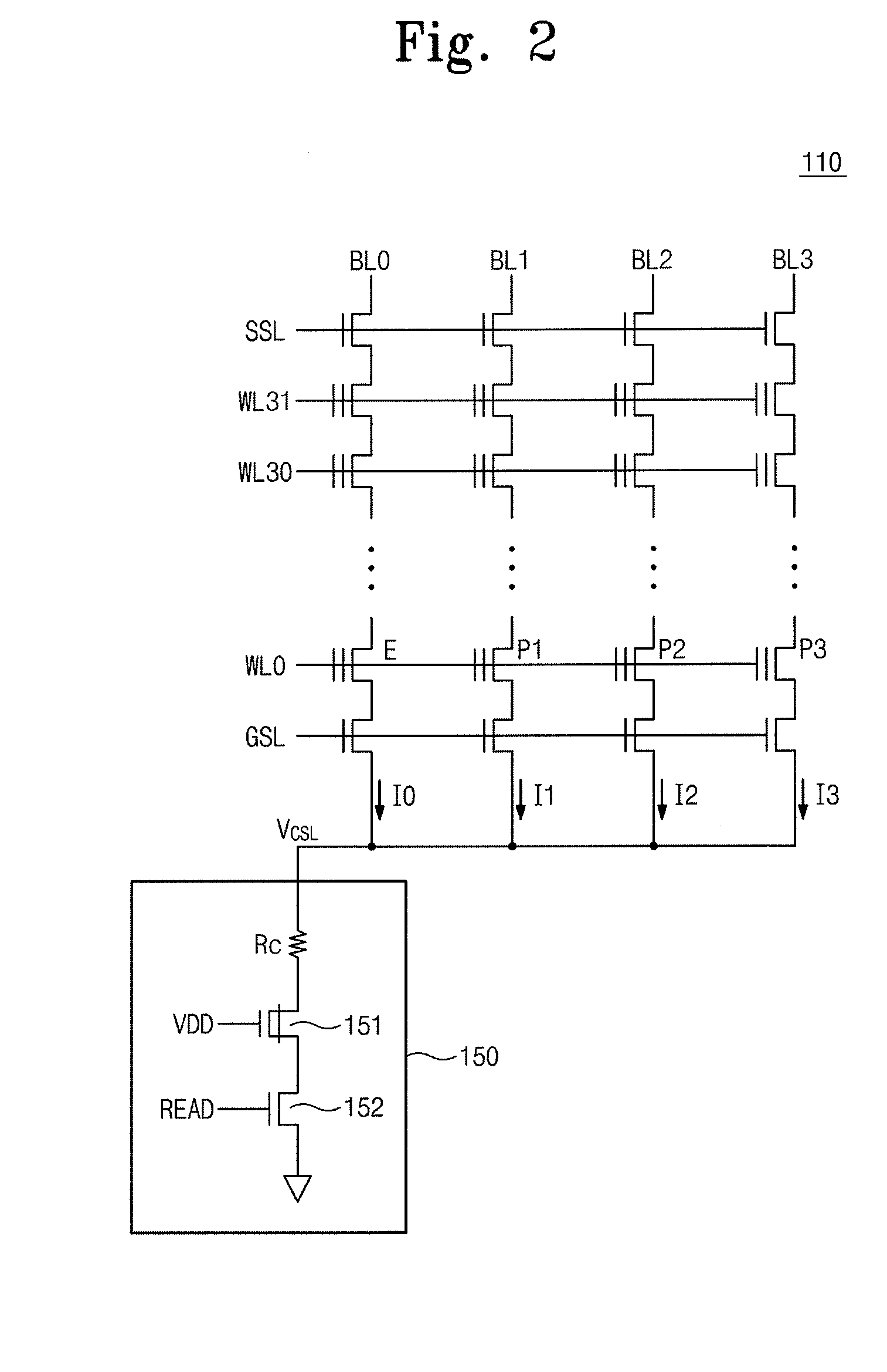
[0028]FIG. 1 is a block diagram of a flash memory device according to an exemplary embodiment of the present invention. Referring to FIG. 1, the flash memory device 100 includes a memory cell array 110, a data input / output circuit 120, a row decoder 130, a control logic 140, and a CSL driver 150.

[0029]The memory cell array 110 includes a plur...


PUM


Abstract

A flash memory device controls a common source line voltage and performs a program verify method. A plurality of memory cells is connected between a bit line and the common source line. A data input/output circuit is connected to the bit line and is configured to store data to be programmed in a selected memory cell of the plurality of memory cells. The data input/output circuit maintains data to be programmed within the data input/output circuit during a program verify operation, and decreases noise in the common source line by selectively precharging the bit line based on the data to be programmed.

Description

CROSS REFERENCE TO RELATED APPLICATIONS[0001]This application claims priority under 35 U.S.C § 119 to Korean Patent Application No. 10-2008-0065114, filed on Jul. 4, 2008, in the Korean Intellectual Property Office, the entire contents of which are herein incorporated by reference.BACKGROUND[0002]1. Technical Field[0003]The present invention is related to a flash memory device, and more particularly, to a flash memory device capable of reducing noise in common source line, a program verify method thereof, and a memory system including the same.[0004]2. Discussion of Related Art[0005]The semiconductor memory device may be generally divided into a volatile memory device, for example, DRAM and SRAM, and a non-volatile memory device, for example, EEPROM, FRAM, PRAM, MRAM and flash memory. A volatile memory device loses stored data when power supply is cut off, but a nonvolatile memory device retains stored data even when power supply is cut off. A flash memory has characteristics such a...

Claims


Application Information

Patent Timeline
IPC IPC(8): G11C16/04G11C16/06G11C7/10
CPCG11C7/02G11C7/1048G11C2211/5642G11C16/0483G11C2211/5621G11C11/5628G11C16/34G11C16/24G11C16/08
Inventor KANG, SANG-GULEE, HEE-WONLEE, JU-SEOKSONG, JUNG-HO
Owner SAMSUNG ELECTRONICS CO LTD
Why Eureka
Try Eureka