Unlock instant, AI-driven research and patent intelligence for your innovation.

Tft-lcd array substrate and manufacturing method thereof

Inactive Publication Date: 2010-01-21
BEIJING BOE OPTOELECTRONCIS TECH CO LTD
View PDF0 Cites 18 Cited by
  • Summary
  • Abstract
  • Description
  • Claims
  • Application Information

AI Technical Summary

Benefits of technology

[0003]One 3-mask process has been proposed in Chinese patent application CN 200510132423.X, in which a gate line and a gate electrode are formed through a patterning process with a first normal mask; a data line, a source electrode, a drain electrode, and a thin film transistor (TFT) channel region are then formed through a patterning process with a second gray tone mask; and a pixel electrode is finally formed through a patterning process with a third normal mask. In the third patterning process of this method, a transparent conductive film is directly formed on the surface of the photoresist for patterning by sputtering, and then the transparent pixel electrode is formed with directly contacting with the surface of the drain electrode by lifting off. In practice, the photoresist is prone to be modified during the sputtering process, thus the pixel region can be polluted and formation of the transparent conductive film by sputtering can fail. Furthermore, the pixel electrode performance is very important to the whole TFT-LCD array substrate and has a great influence on the display quality. Therefore, it is needed that the 3-mask process is improved so as to avoid the problems mentioned above.

Problems solved by technology

In practice, the photoresist is prone to be modified during the sputtering process, thus the pixel region can be polluted and formation of the transparent conductive film by sputtering can fail.

Method used


Image

  • Tft-lcd array substrate and manufacturing method thereof
  • Tft-lcd array substrate and manufacturing method thereof
  • Tft-lcd array substrate and manufacturing method thereof

Examples


first embodiment

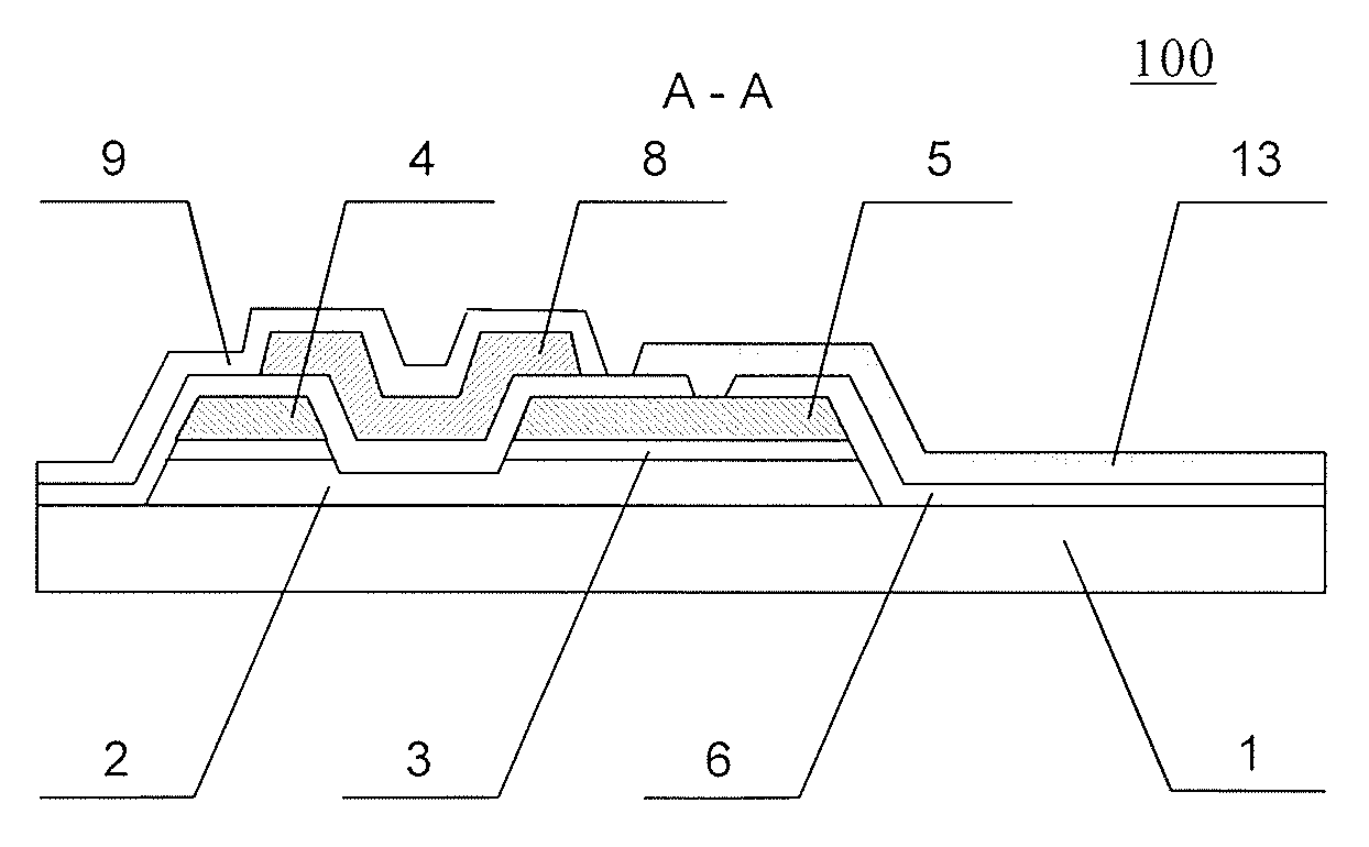
[0040]FIG. 1 is a schematic view showing a structure of a TFT-LCD array substrate according to the present invention; and FIG. 2 is a sectional view taken along a line A-A in FIG. 1. For example, the array substrate 100 of the present embodiment comprises a plurality of data lines 11 and a plurality of gate lines 12 perpendicular to and insulated from the date lines on a base substrate 1, a plurality of pixel regions are defined by the intersections between the data lines 11 and the gate lines 12, thin film transistors (TFTs) are each formed at the intersections for the pixel regions, and pixel electrodes 13 are each formed in the pixel regions. Each TFT of the present embodiment for example comprises a semiconductor layer 2 and a doped semiconductor layer 3 formed on the base substrate 1, a source electrode 4 and a drain electrode 5 formed on the doped semiconductor layer 3, a TFT channel region formed between the source electrode 4 and the drain electrode 5, a first insulating lay...

second embodiment

[0073]A method for manufacturing a TFT-LCD array substrate according to the present invention comprises the following steps:

[0074]Step 1′ of depositing a light-shielding layer, a semiconductor layer, a doped semiconductor layer and a metal film for source and drain electrodes sequentially on a base substrate and then forming a data line, a source electrode, a drain electrode and a thin film transistor (TFT) channel region by a first patterning process;

[0075]Step 2′ of depositing a first insulating film and a gate metal film sequentially on the substrate after the step 1′ and then forming a gate line and a gate electrode by a second patterning process and forming an insulating layer via hole in the first insulating layer above the drain electrode;

[0076]Step 3′ of depositing a transparent conductive film on the substrate after the step 2′ and then forming a pixel electrode by a third patterning process, which is connected with the drain electrode through the insulating layer via hole;...


PUM


Abstract

A liquid crystal display (LCD) array substrate and a manufacturing method thereof are provided. The manufacturing method comprises depositing a semiconductor layer, a doped semiconductor layer and a metal film for source and drain electrodes sequentially on a base substrate and then forming a data line, a source electrode, a drain electrode and a thin film transistor (TFT) channel region by a first patterning process; depositing a first insulating film and a gate metal film sequentially and then forming a gate line and a gate electrode by a second patterning process and forming an insulating layer via hole in the first insulating layer above the drain electrode; depositing a transparent conductive film and then forming a pixel electrode by a third patterning process; and forming a second insulating layer.

Description

BACKGROUND[0001]Embodiments of the present invention relate to a liquid crystal display array substrate (LCD) and a manufacturing method thereof.[0002]Thin film transistor liquid crystal displays (TFT-LCDs) possess advantages of small volume, low power consumption, low radiation, etc., and are gradually prevailing in the market of flat plate displays. As for a TFT-LCD, an array substrate and the manufacturing method thereof control, to a large extent, the performance, yield, and price of the final products. In order to efficiently reduce the production cost of TFT-LCDs and improve yield, the manufacturing process of a TFT-LCD array substrate is gradually simplified. Such manufacturing processes have been evolving from initial 7-mask processes to current 4-mask processes for example based on slit photolithography technology. Besides, 3-mask processes are under research and development.[0003]One 3-mask process has been proposed in Chinese patent application CN 200510132423.X, in which...

Claims


Application Information

Patent Timeline
IPC IPC(8): H01L33/00
CPCH01L27/1288G02F1/1368
Inventor ZHI, HOUJUNG, JAE YUNZHENG, YUNYOUXIAO, HONGXILI, WEI
Owner BEIJING BOE OPTOELECTRONCIS TECH CO LTD