Light emitting device

a technology of light-emitting devices and wires, which is applied in the direction of semiconductor devices, basic electric elements, electrical equipment, etc., can solve the problems of large stress applied to electrical connection members such as wires, and prevent wire disconnection, and reduce the stress applied to wires for wire bonding. , the effect of low shore hardness

Active Publication Date: 2010-02-04
TOYODA GOSEI CO LTD
View PDF14 Cites 57 Cited by
  • Summary
  • Abstract
  • Description
  • Claims
  • Application Information

AI Technical Summary

Benefits of technology

[0029]According to one embodiment of the invention, a light emitting device is constructed such that it uses a sealing material with a relatively low shore hardness A. Therefore, stress applied to wires for wire bonding can be relatively small such that wire disconnection can be prevented ev...

Problems solved by technology

However, the light emitting device of JP-A-2002-314142 has the problem that stress applied to an electrical connection member such as wires becomes relatively large since it uses the s...

Method used


Image

  • Light emitting device
  • Light emitting device
  • Light emitting device

Examples


first embodiment

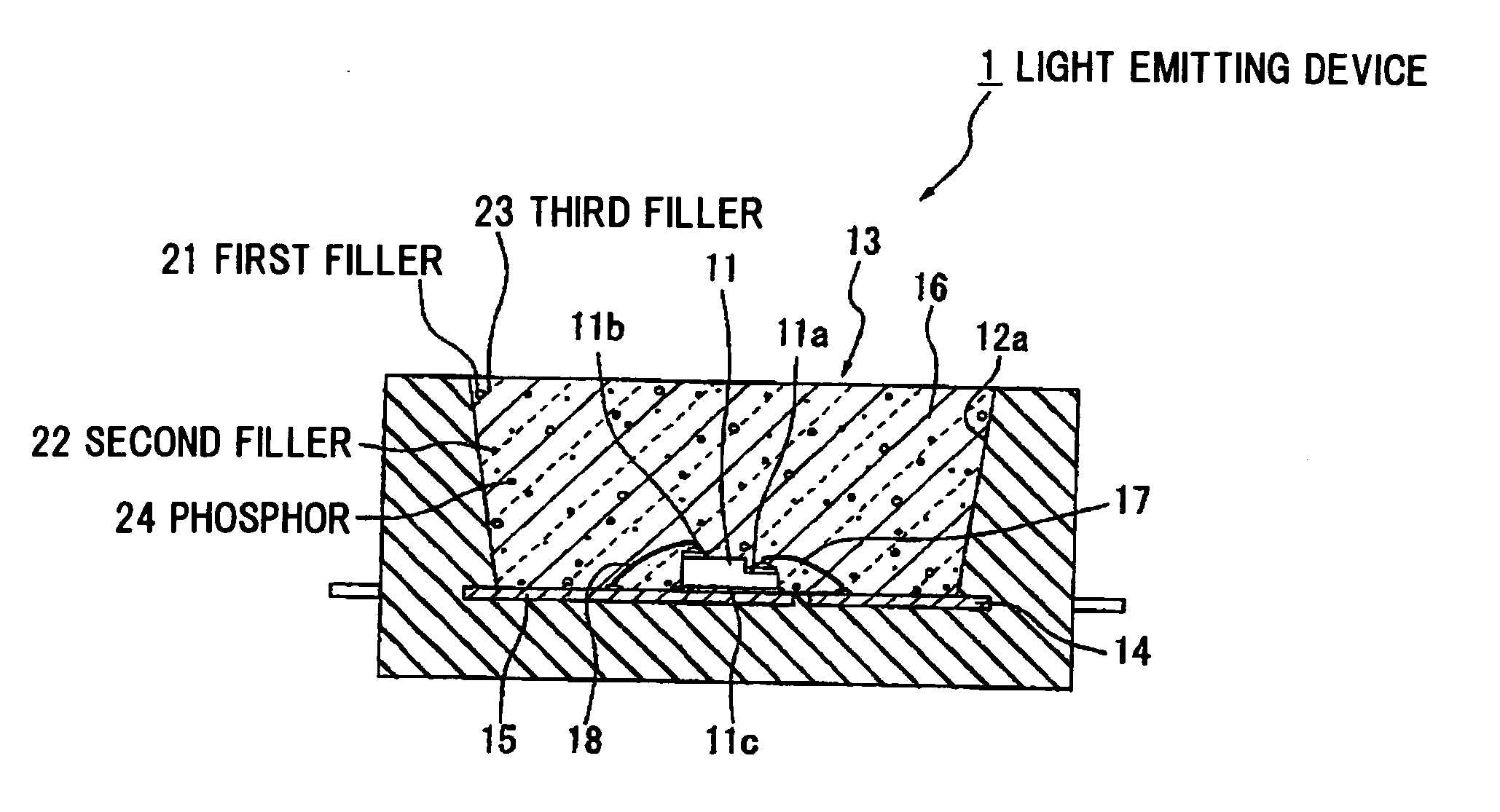
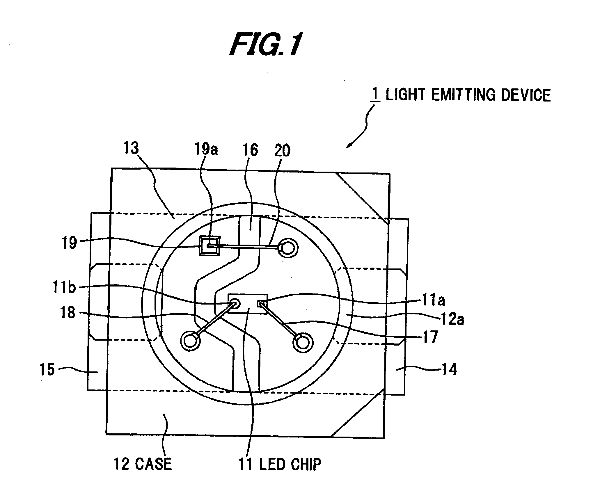
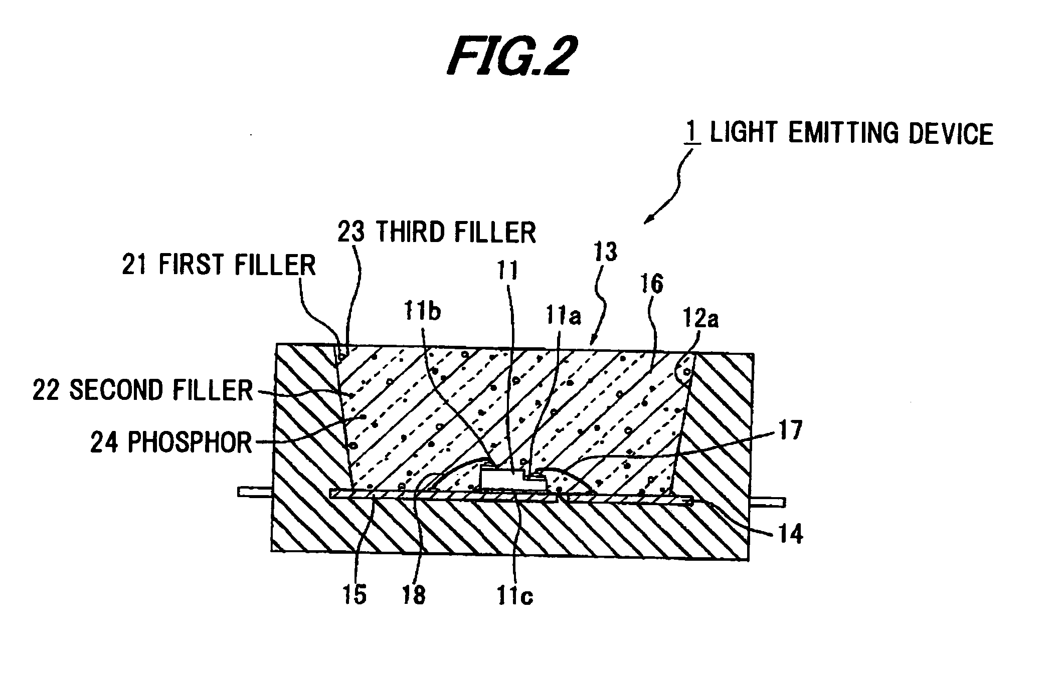
[0035]FIGS. 1 and 2 show a light emitting device of the first embodiment, where FIG. 1 is a top view showing the light emitting device and FIG. 2 is a cross sectional view showing the light emitting device.

[0036]As shown in FIG. 1, the light emitting device 1 is composed of an LED (light-emitting diode) chip 11, a case 12 of a resin material and with a concave portion 13 that includes a reflector portion 12a surrounding the LED chip 11, a first lead 14 and a second lead 15 that are exposed at the bottom of the concave portion 13 of the case 12 and disposed separately from each other in the horizontal direction, and a sealing material 16 that is filled in the concave portion 13 and formed of a resin. The light emitting device 1 is further composed of a first wire 17 for connecting one electrode 11a with the first lead 14, a second wire 18 for connecting the other electrode with the second lead 15, a Zener diode 19 as a protective element, and a third wire 20 for connecting an electro...


PUM


Abstract

A light emitting device includes a light emitting element, a sealing material for sealing the light emitting element, a first filler included in the sealing material, and a second filler included in the sealing material. The second filler includes a particle diameter smaller than that of the first filler.

Description

[0001]The present application is based on Japanese patent application No. 2008-194903 filed on Jul. 29, 2008, the entire contents of which are incorporated herein by reference.BACKGROUND OF THE INVENTION[0002]1. Field of the Invention[0003]This invention relates to a light emitting device that a light emitting element is sealed with a sealing member.[0004]2. Description of the Related Art[0005]A light emitting device is disclosed which is composed of a light emitting device for emitting a primary light, silicone formed to cover a light emitting element and having a hardness of more than 50 in JISA value, and a phosphor for absorbing the primary light and emitting a visible light (See JP-A-2002-314142).[0006]However, the light emitting device of JP-A-2002-314142 has the problem that stress applied to an electrical connection member such as wires becomes relatively large since it uses the sealing resin with a relatively high hardness. In other words, the large stress applied to the el...

Claims


Application Information

Patent Timeline
IPC IPC(8): H01L33/00
CPCH01L33/56H01L2933/0091H01L2224/48091H01L2224/49107H01L2224/73265H01L2224/16245H01L2224/73204H01L2924/00014H01L2224/04042
Inventor KOSEKI, MASAKATAKAWANO, EIKI
Owner TOYODA GOSEI CO LTD
Why Eureka
Try Eureka