Plasma source and methods for depositing thin film coatings using plasma enhanced chemical vapor deposition

a technology of plasma and chemical vapor deposition, which is applied in the field of plasma source for plasma enhanced chemical vapor deposition (cvd), can solve the problems of difficult implementation of pecvd applied to large area coating, drawbacks of using the above-mentioned pecvd apparatuses for coating large area surfaces, and large volume of magnetron sources, etc., and achieves high secondary electron current, high plasma current, and high reactivity

Active Publication Date: 2010-02-04
AGC FLAT GLASS NORTH AMERICA INC +1
View PDF31 Cites 115 Cited by
  • Summary
  • Abstract
  • Description
  • Claims
  • Application Information

AI Technical Summary

Benefits of technology

[0016]In an aspect of the invention, there is provided a stable, uniform and long plasma.
[0017]In an aspect of the invention, there is provided a plasma source that is able to form a stable, uniform and long plasma.

Problems solved by technology

Thus, PECVD applied to large area coating has been difficult to implement.
However, there are drawbacks associated with using the aforementioned PECVD apparatuses for coating large area surfaces.
Magnetron sources, for example, tend to quite bulky, typically 150 mm wide by 300 mm deep, and require magnets.
Also, when used for PECVD, the surface of a magnetron source tends to become coated with the material being deposited, and thus, the magnetron becomes insulated, which can lead to arcing and other complications.
Furthermore, the sputtered material contaminates the material being deposited.
Anode ion layer sources, for example, suffer from similar drawbacks as magnetron sources in that they tend to be bulky, require magnets, as well as become coated.
Madocks sources, for example, suffer from the drawbacks of being bulky and requiring magnets, as well as low coating efficiencies, about 15%.
However, U.S. Pat. No. 6,444,945 does not address the use of the disclosed hollow cathodes for any PECVD process or for large area surface coating.

Method used


Image

  • Plasma source and methods for depositing thin film coatings using plasma enhanced chemical vapor deposition
  • Plasma source and methods for depositing thin film coatings using plasma enhanced chemical vapor deposition
  • Plasma source and methods for depositing thin film coatings using plasma enhanced chemical vapor deposition

Examples


example 1

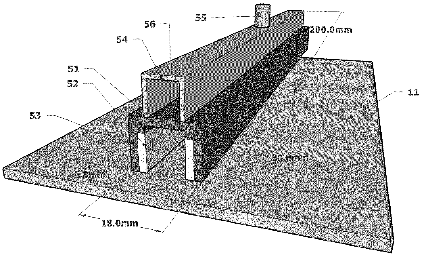
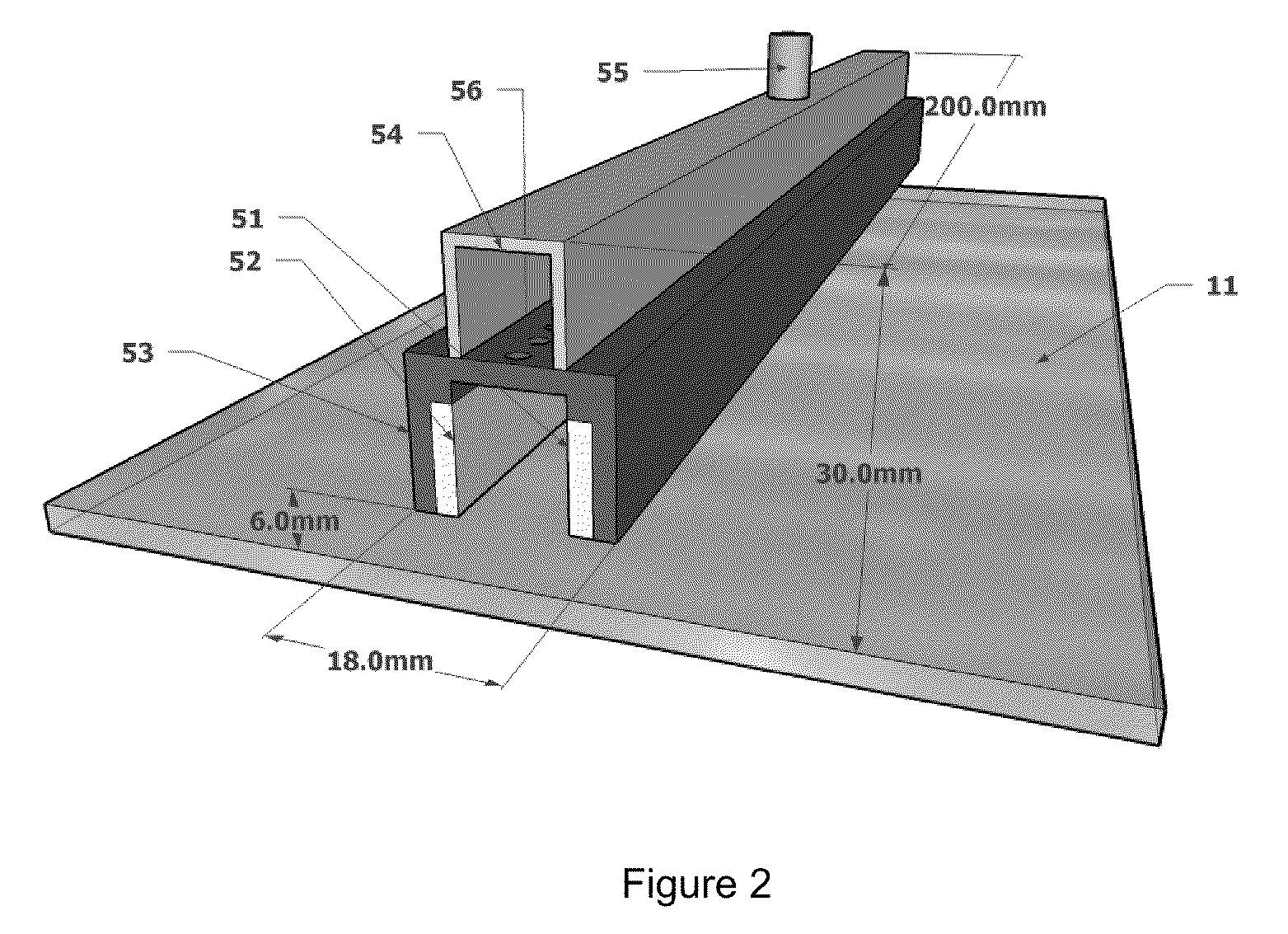
[0112]A silicon dioxide coating made from the PECVD device of FIG. 5 is described below. The PECVD device has a total length of about 150 mm and a width of about 50 mm. The distance from the bottom of the hollow cathode electrodes to a top surface of a glass substrate was fixed at 11 mm. A total of four hollow cathodes were disposed adjacently and connected to an AC power source. Precursor gas was supplied to dark space 33 via feed tubes 36 and was supplied at a rate of 100 sccm. The precursor gas was 100% tetramethyldisiloxane. Reactant gas was supplied to the hollow cathode space via feed tubes 35. The reactant gas was 100% oxygen and was supplied at a rate of 300 sccm. Substrate 11 was a piece of soda-lime float glass and was held stationary under the PECVD source of FIG. 5. The AC power supply source used was an Advanced Energy PE-II, 40 kHz AC power supply source. The size of the coated area on substrate 11 was 50 mm×100 mm. Results of the coating process are given in Table 1.

T...


PUM

PropertyMeasurementUnit
lengthaaaaaaaaaa
lengthaaaaaaaaaa
temperatureaaaaaaaaaa

Abstract

The present invention provides novel plasma sources useful in the thin film coating arts and methods of using the same. More specifically, the present invention provides novel linear and two dimensional plasma sources that produce linear and two dimensional plasmas, respectively, that are useful for plasma-enhanced chemical vapor deposition. The present invention also provides methods of making thin film coatings and methods of increasing the coating efficiencies of such methods.

Description

CROSS REFERENCE TO RELATED APPLICATION[0001]This application claims the benefit of U.S. Provisional Application No. 61 / 137,839, filed Aug. 4, 2008, which is hereby incorporated by reference in its entirety into the present application.BACKGROUND OF THE INVENTION[0002]1. Field of the Invention[0003]The present invention relates generally to a plasma source for deposition of thin films and chemical modification of surfaces. More particularly, the present invention relates to a linear plasma source for plasma enhanced chemical vapor deposition (CVD).[0004]2. Discussion of the Background[0005]All United States Patents and Patent Applications referred to herein are hereby incorporated by reference in their entireties. In the case of conflict, the present specification, including definitions, will control.[0006]The deposition of thin films can be accomplished by many techniques, the most common including chemical deposition, physical deposition and mixtures of the two. For chemical deposi...

Claims


Application Information

Patent Timeline
Patent Type & Authority Applications(United States)
IPC IPC(8): C01B33/12C23C16/513H05H1/24
CPCC23C16/402C03C2218/153C23C16/503H01J37/32568H01J37/3266H01J37/32724H05H1/24H01J2237/3321H01J2237/3328C23C16/513H01J37/32036H01J37/32596C03C17/245C03C17/2456C03C2217/213C23C16/45517H05H1/42H05H1/46H05H1/466
Inventor MASCHWITZ, PETER
Owner AGC FLAT GLASS NORTH AMERICA INC
Why Eureka
Try Eureka