Cache system, cache system control method, and information processing apparatus
a cache system and control method technology, applied in the direction of memory address/allocation/relocation, instruments, computing, etc., can solve the problems of degrading the performance of the cache, increasing the power consumption of the cache memory in the power consumption of the microprocessor, and invalidating cache data stored in the way
- Summary
- Abstract
- Description
- Claims
- Application Information
AI Technical Summary
Benefits of technology
Problems solved by technology
Method used
Image
Examples
first embodiment
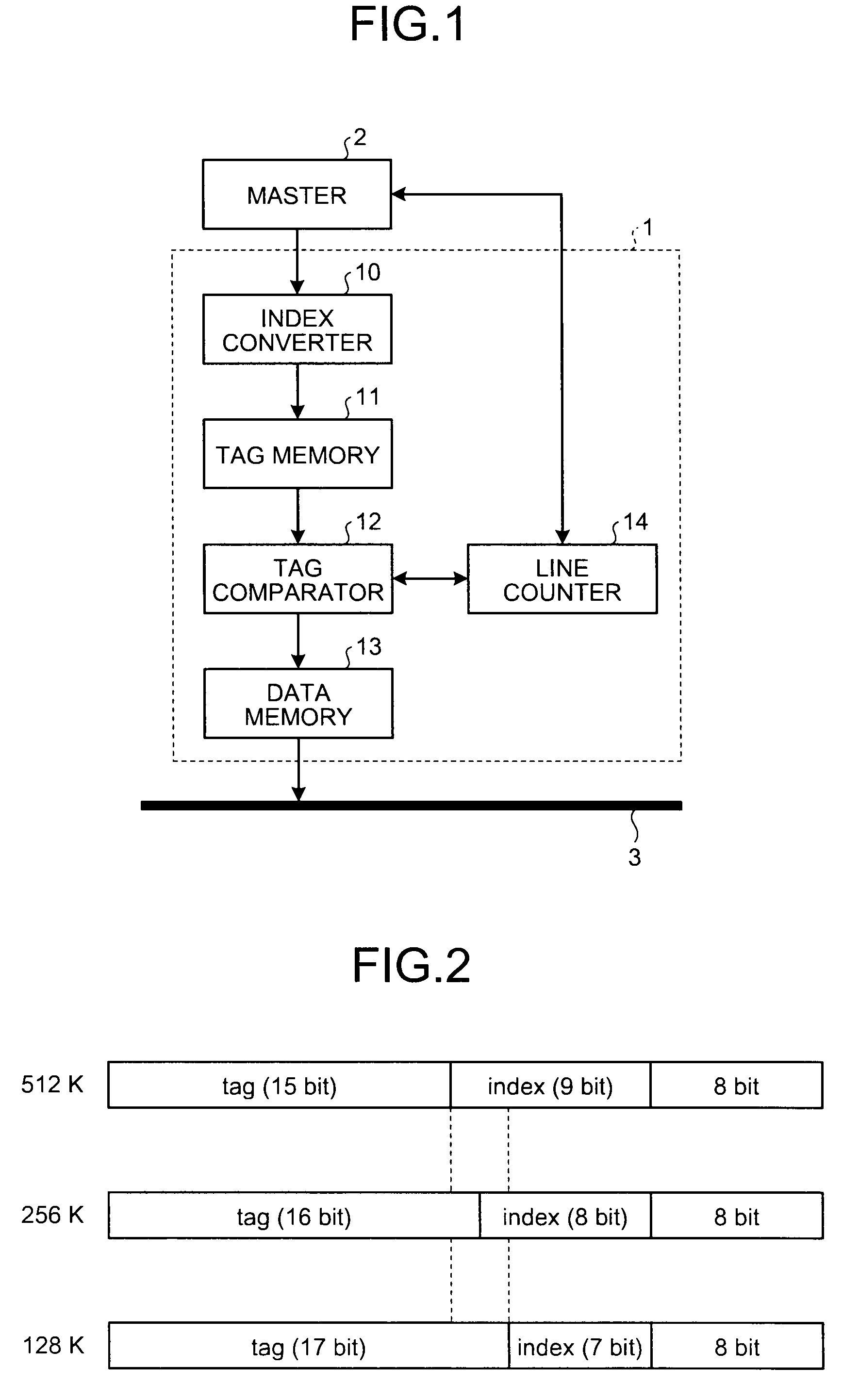
[0022]FIG. 1 is a block diagram of a schematic configuration of an information processing apparatus having a cache system 1 according to the present invention. The information processing apparatus includes the cache system 1, a master 2, a bus 3, and a main memory. The cache system 1 includes a data cache memory, and adopts, for example, a 4-way set associative system. The master 2 can be a processor or a hard engine that accesses the cache system 1. The cache system 1 is connected to the main memory via the bus 3.
[0023]The cache system 1 can be incorporated in the chip or externally attached thereto, and can be used for any hierarchy of, for example, L1 cache (Level 1 Cache), L2 cache (Level 2 Cache), and L3 cache (Level 3 Cache). Further, the cache system 1 can be appropriately transformed based on the outline explained below, by persons skilled in the corresponding technique. For example, the cache system 1 can be also transformed to any system adopting associativity of an n-way ...
second embodiment
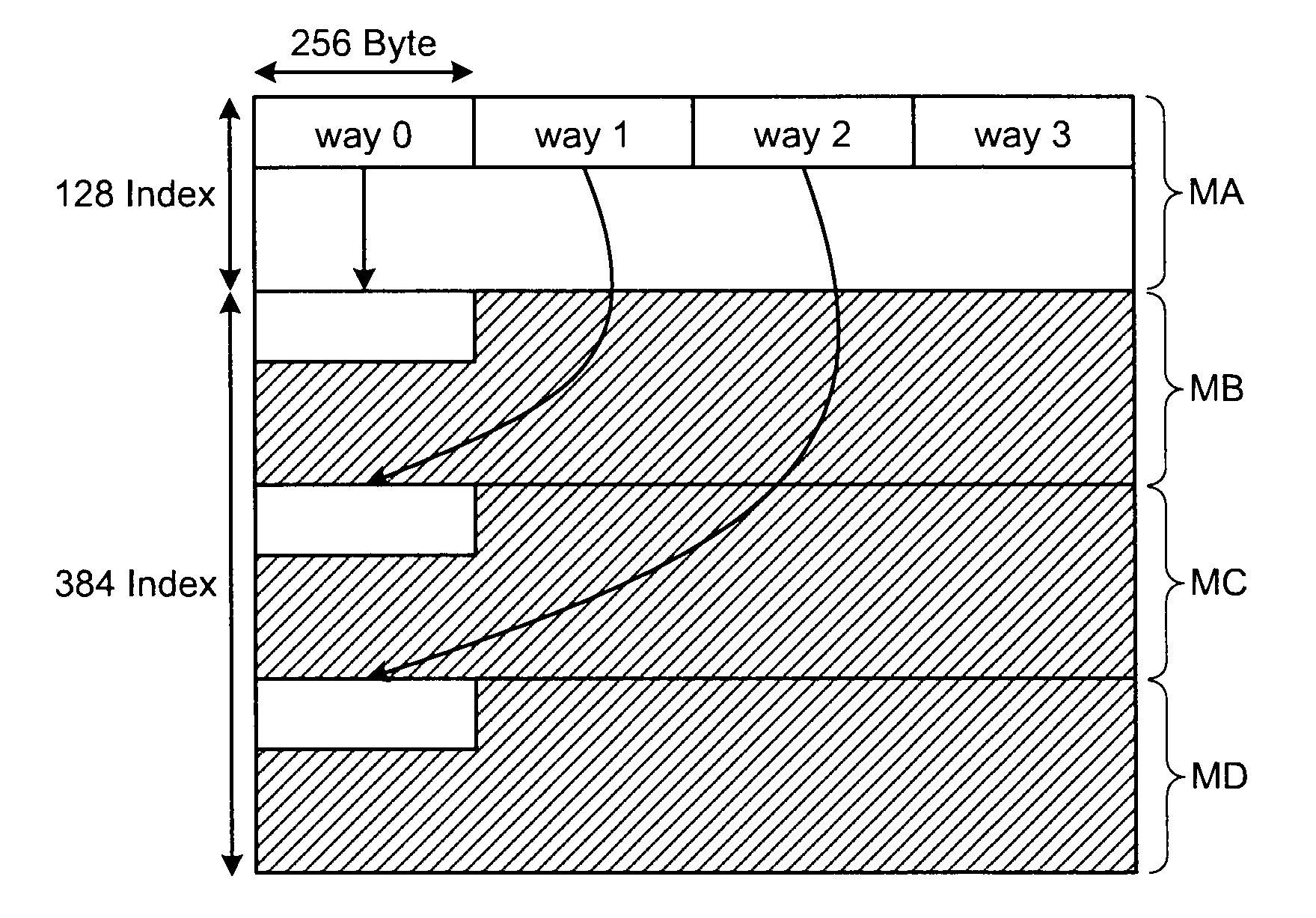
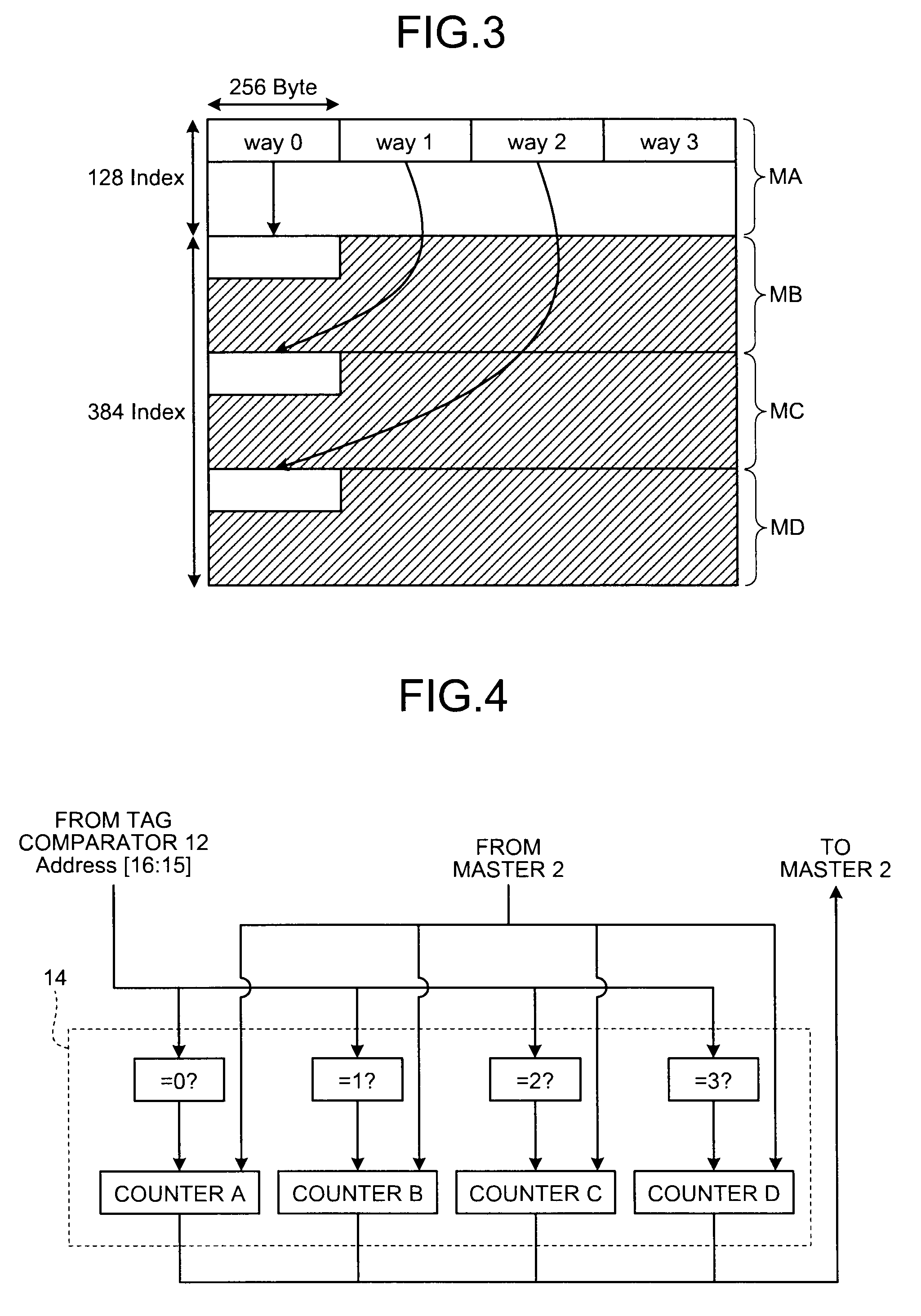
[0053]For example, when the cache capacity is to be decreased from 512 Kbytes to 128 Kbytes, as shown in FIG. 5, it is assumed that the counted number of the counter A in the line counter 14 is “18”, the counted number of the counter B is “45”, the counted number of the counter C is “30”, and the counted number of the counter D is “38”. Also in this case, pieces of the cache data to be arranged in the memory areas MA, MC, and MD to which the counter A, the counter C, and the counter D are respectively allocated, other then the counter B having the largest counted number, are to be invalidated. Also in the second embodiment, an operation requiring the least write back processing can be selected, thereby enabling to reduce the time required for changing the cache capacity.
[0054]FIG. 9 is a schematic diagram for explaining the arrangement of the cache data after the cache capacity has been changed from 512 Kbytes to 128 Kbytes. After the invalidation process, the cache system 1 uses on...
third embodiment
[0057]In the third embodiment, the counter A, the counter B, the counter C, and the counter D in the line counter 14 respectively increment the counted number by one every time data is refilled in the cache line from the lower-order memory, and decrement the counted number by one every time the cache data stored in the cache line is released (flushed). As a condition for decrementing the counted number by one, it is not considered whether there is write-back of data from the cache line to the lower-order memory.
[0058]The counted number of the counter A expresses the number of effective lines, in which the cache data is arranged in memory area MA (indexes 0 to 127) when the cache capacity is maximum 512 Kbytes. The counted number of the counter B expresses the number of effective lines, in which the cache data is arranged in memory area MB (indexes 128 to 255) when the cache capacity is maximum 512 Kbytes. The counted number of the counter C expresses the number of effective lines, i...
PUM
 Abstract
Description
Claims
Application Information


