
Liquid crystal display with light emitting diode backlight assembly and liquid crystal display thereof

Inactive Publication Date: 2010-02-18
SAMSUNG DISPLAY CO LTD
View PDF6 Cites 33 Cited by
  • Summary
  • Abstract
  • Description
  • Claims
  • Application Information

AI Technical Summary

Benefits of technology

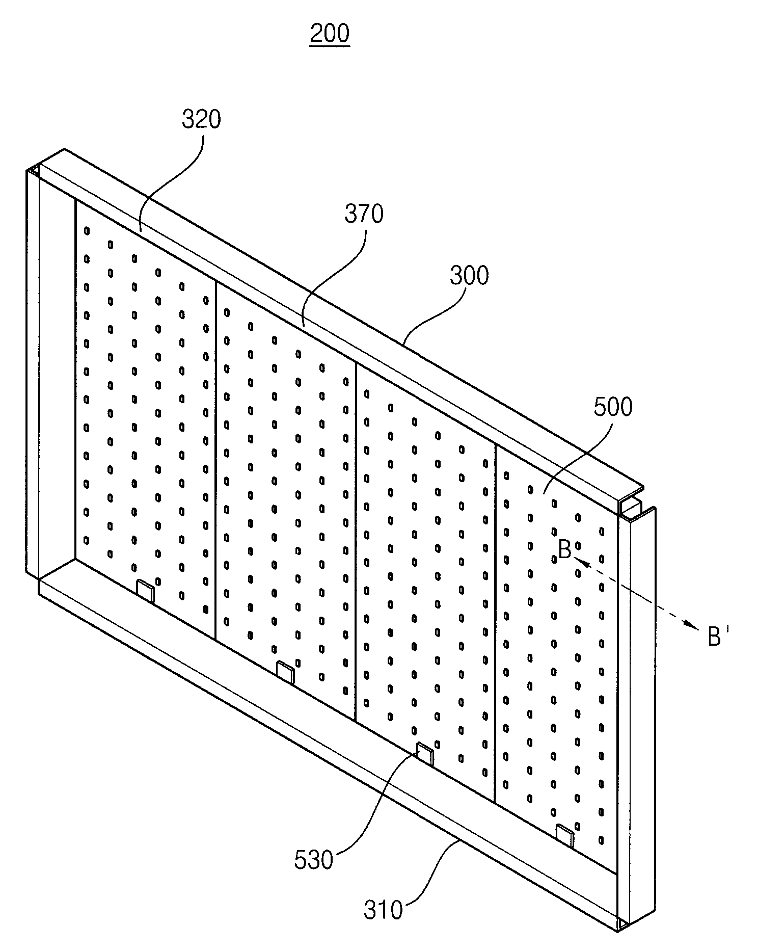
[0012]Thus, it is an aspect of the disclosure to provide an improve LED backlight assembly wherein the location of the LED-PCB connector, location of the LED driving board, and structure of the bottom frame are designed to make the LCD compact and easy to assemble.
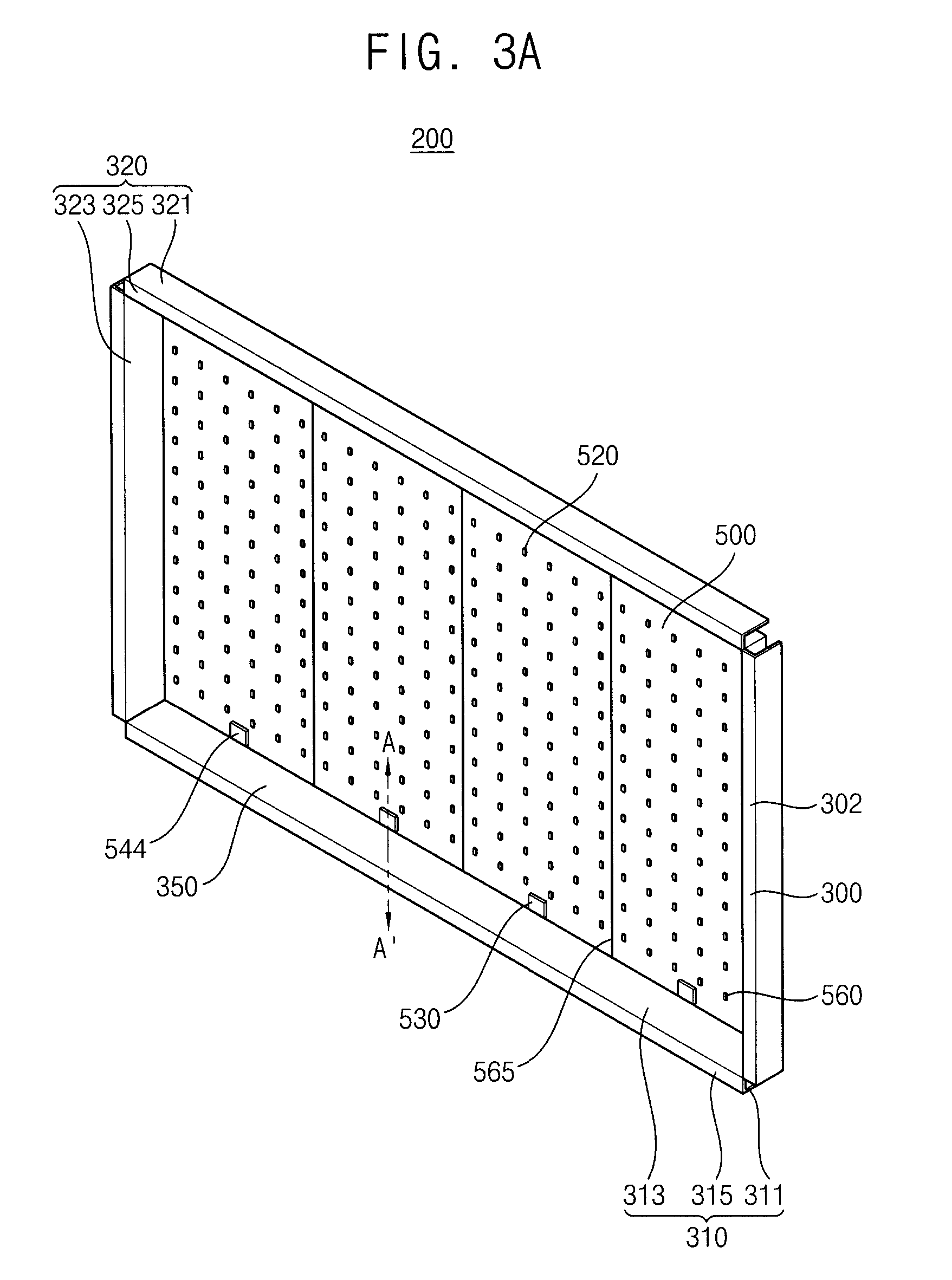
[0021]According to yet another embodiment, the light emitting diode backlight assembly has a plurality of light emitting diode printed circuit boards which are aligned vertically. That is, the longer side of the light emitting diode printed circuit board is orthogonal to the longer edge of a bottom container of the light emitting diode backlight assembly. Accordingly, light emitting diode printed circuit board connector of each light emitting diode printed circuit board is located in the vicinity of the longer edge and connected to a light emitting diode driving board located within or near the longer edge of the bottom container. Then, an electrical cable connects the light emitting diode driving board and each light emitting diode printed circuit board connector without changing an extension direction vertically, thereby simplifying assembly.

Problems solved by technology

Since the LED driving board is fixed on a different side from the LED-PCB, the cable is very lengthy and its connection to both the LED driving board and LED-PCB is very difficult.
Still further, the edge and outwardly located LED-PCB connector makes the backlight assembly and the LCD bulky, especially in a top plan plane view.

Method used


Image

  • Liquid crystal display with light emitting diode backlight assembly and liquid crystal display thereof
  • Liquid crystal display with light emitting diode backlight assembly and liquid crystal display thereof
  • Liquid crystal display with light emitting diode backlight assembly and liquid crystal display thereof

Examples


Embodiment Construction

[0038]Reference will now be made in further detail to exemplary embodiments, examples of which are illustrated in the accompanying drawings, wherein like reference numerals refer to like elements throughout. The embodiments are described below in order to explain the embodiments by referring to the figures.

[0039]The terms “the”, “a” and “an” do not denote a limitation of quantity, but rather denote the presence of at least one of the referenced item. The suffix “(s)” as used herein is intended to include both the singular and the plural of the term that it modifies, thereby including at least one of that term (e.g., the “LED”(s) includes at least one “LED”).

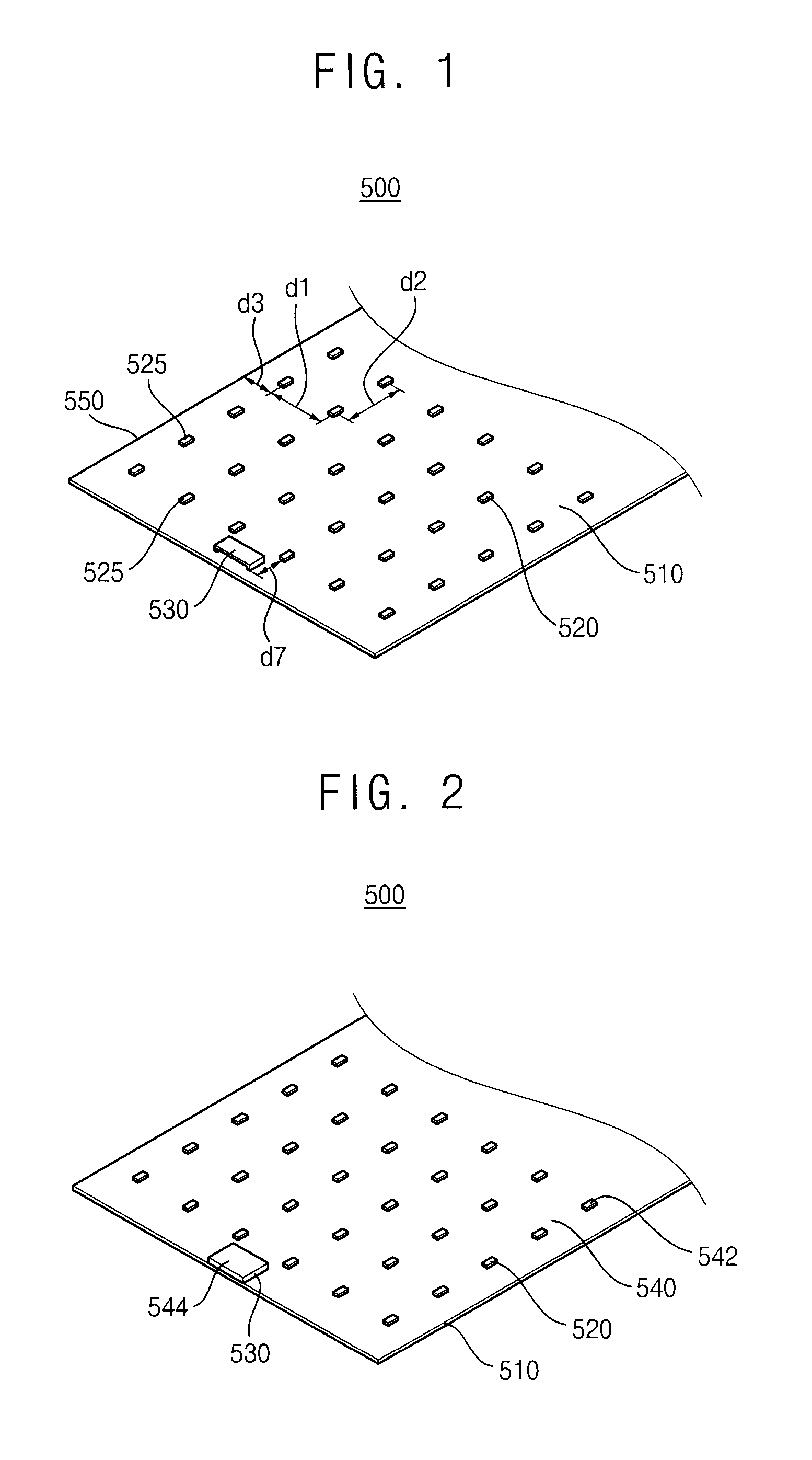
[0040]FIG. 1 is a perspective view of an LED-PCB comprising a plurality of LEDs and an LED-PCB connector placed at an end portion of the LED-PCB. Referring to FIG. 1, an LED-PCB 500 is provided with a printed circuit board (“PCB”) 510, a plurality of LEDs 520 and an LED-PCB connector 530. Here, the PCB provides electrical connect...


PUM

PropertyMeasurementUnit
Thicknessaaaaaaaaaa
Structureaaaaaaaaaa
Distanceaaaaaaaaaa

Abstract

A light emitting diode (“LED”) backlight assembly. The LED backlight assembly has a bottom container which has a bottom plate and a side edge surrounding the bottom plate, a plurality of light emitting diode printed circuit boards (“LED-PCBs”) on the bottom plate, and a connector which is closely located to edge located LEDs. The connector of the LED-PCB is closely located to an LED driving board, which is disposed at a lateral space of a lateral part of the bottom container to limit a vertical thickness of the backlight light assembly.

Description

[0001]This application claims priority to Korean patent Application No. 2008-78899, filed on Aug. 12, 2008, and all the benefits accruing therefrom under 35 U.S.C. §119, the contents of which in its entirety are herein incorporated by reference.BACKGROUND OF THE INVENTION[0002](1) Field of the Invention[0003]This disclosure relates to a liquid crystal display (“LCD”) with a light emitting diode (“LED”) backlight assembly, and more particularly, to the LED backlight assembly having an LED driving board disposed at a lateral part of a bottom container of the LED backlight assembly.[0004](2) Description of the Related Art[0005]As display devices are used in everyday life, the liquid crystal display (“LCD”) has been gaining in popularity. To display an image, the LCD has both a liquid crystal (“LC”) panel and a backlight assembly The backlight assembly emits light, while the LC panel receives the light from the backlight assembly and displays an image by selectively allowing light from ...

Claims


Application Information

Patent Timeline
IPC IPC(8): G02F1/1333F21S4/00F21V7/00G09F13/04H05K3/10
CPCG02F1/133603Y10T29/49128Y10T29/49155G02F1/133608G02F2001/133612H05K1/148G02F1/133612G02F1/1333G02F1/1335
Inventor PARK, JIN-HEELEE, YONG-WOOKIM, WON-JUKIM, YONG-IL
Owner SAMSUNG DISPLAY CO LTD
Learn More