

Printed circuit board and method of producing the same
- Summary
- Abstract
- Description
- Claims
- Application Information
AI Technical Summary
Benefits of technology
Problems solved by technology
Method used
Image

Examples
first embodiment
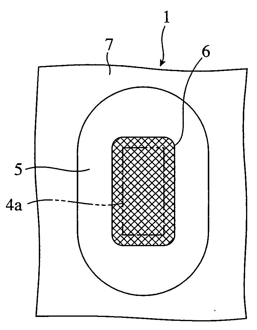
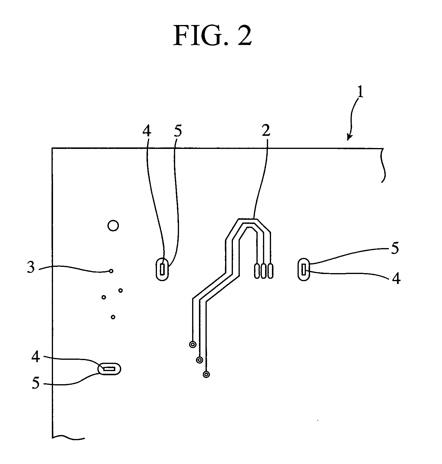
[0016]FIG. 1(A) shows a fragmentary plan view of a hole-forming portion of a printed circuit board according to the first embodiment of the present invention, and FIG. 1(B) shows a fragmentary plan view of the board after completion of a hole-forming process. FIG. 2 shows a fragmentary plan view of the printed circuit board by way of example.
[0017]As shown in FIG. 2, formed through a printed circuit board 1 are formed non-conductive holes 4 for mounting a component and having corners, in addition to wirings 2 and through holes 3. The holes having corners include a hole having a curved portion or edge on one end side thereof and corners on the other end side and a hole shaped like a cross, in addition to a rectangular hole shown in the figure by way of example. An explanation will be given by referring to a hole having a corner simply as a “hole” hereinafter. In the place of the board 1 where a hole 4 is to be formed, as shown in FIG. 1(A), a patternless section 6 without a cupper fo...
second embodiment
[0020]FIG. 3(A) shows a fragmentary plan view of a printed circuit board according to the second embodiment, and FIG. 3(B) shows a fragmentary plan view of the board after completion of a hole-forming process.
[0021]In the place of a board 1 where a hole 4 is to be formed, four areas corresponding to the corner areas of the hole 4 within a land (wiring pattern) 5 formed of copper foil are each provided with a circular patternless section 11 having no copper foil. The patternless section 11 is located in each of the corner areas of the outline 4a (shown by the chain double-dashed line in the figure) of the hole 4 to be formed. Therefore, when in the sections, the board is subjected to a hole-forming process by punching using a die press or the like, the hole 4 formed therethrough does not have any land 5, that is, any copper foil portion in each of its corner areas as shown in FIG. 3(B), and thus any burr is not left in the corner areas of the hole 4.
[0022]In the manufacturing of a bo...
third embodiment
[0024]FIG. 4(A) shows a fragmentary plan view of a printed circuit board according to the third embodiment, and FIG. 4(B) shows a fragmentary plan view of the board after completion of a hole-forming process. The third embodiment is applied to a hole 21, which is not rectangular, has a corner area in some places, and has a curved edge or portion in other places.
[0025]As shown in FIG. 4(A), in the place of a board 1 where the hole 21 is to be formed, the areas corresponding to the two corner areas of the hole 21 are each provided with a patternless section 23 that is circular and does not have a copper foil. The patternless section 23 is located in each of the corner areas of the outline 21a (shown by the chain double-dashed line in the figure) of a hole to be formed. For this reason, when in the sections, the board is subjected to a punching process with a die press or the like, the hole 21 formed therethrough does not have any land 22, that is, any copper foil in each of the two co...
PUM
| Property | Measurement | Unit |
|---|---|---|
| Electrical conductor | aaaaa | aaaaa |
| Area | aaaaa | aaaaa |
Abstract
Description
Claims
Application Information