Multilayer chip varistor

a multi-layer chip and varistor technology, applied in the direction of varistor, resistor details, current responsive resistors, etc., can solve the problems of connection failure between the internal electrode and the through-hole conductor, and achieve the effect of preventing the connection failure, and preventing the production of cracks

Active Publication Date: 2010-03-04
TDK CORPARATION
View PDF4 Cites 3 Cited by
  • Summary
  • Abstract
  • Description
  • Claims
  • Application Information

AI Technical Summary

Benefits of technology

[0007]An object of the present invention is to provide a multilayer chip varistor capable of suppressing the production of cracks and thereby preventing the connection failure between the internal electrodes and the through-hole conductors.
[0009]In the multilayer chip varistor according to the present invention, at least one of the plurality of internal electrodes is so configured as to be curved toward the direction of penetration of the through hole in the connection portion to the through-hole conductor. When the connection portion is curved toward the direction of penetration of the through hole, a region sandwiched between a curved surface of the connection portion and the through-hole conductor is formed in the varistor layer near the connection portion, on a one-side surface of the internal electrode. This region is sandwiched between the curved surface of the internal electrode and the through-hole conductor. Therefore, metal diffuses into the varistor layer to increase a metal concentration in this region, whereby the contraction percentage of this region in the firing becomes larger than that of the internal electrodes and the through-hole conductor and smaller than that of the varistor layer. Because of this effect, the region with the high metal concentration in the varistor layer acts to relax stress generated in the firing, which suppresses production of cracks originating in the connection portion. Furthermore, the suppression of production of cracks leads eventually to preventing a connection failure between the internal electrode and the through-hole conductor.
[0010]The multilayer chip varistor according to the present invention is preferably so configured that in the internal electrode curved in the connection portion, a thickness in a contact portion with the through-hole conductor is larger than a thickness in a portion other than the connection portion. This configuration increases the area of the contact portion of the internal electrode to the through-hole conductor and thereby further prevents the connection failure between the internal electrode and the through-hole conductor.
[0012]In the multilayer chip varistor according to the present invention, at least one of the plurality of internal electrodes is so configured in the connection portion to the through-hole conductor that the varistor layer is sandwiched between the internal electrode and the through-hole conductor in the direction perpendicular to the direction of penetration of the through hole. In the region of the varistor layer sandwiched between the connection portion of the internal electrode and the through-hole conductor, metal diffuses into the varistor layer to increase a metal concentration. Therefore, the contraction percentage of this region in the firing becomes larger than that of the internal electrodes and the through-hole conductor and smaller than that of the varistor layer. Because of this effect, the region with the high metal concentration in the varistor layer acts to relax stress generated in the firing, which suppresses production of cracks originating in the connection portion. Furthermore, the suppression of production of cracks leads eventually to preventing a connection failure between the internal electrode and the through-hole conductor.

Problems solved by technology

For this reason, the foregoing multilayer chip varistor may suffer cracks originating in the connection portions and the cracks could cause a connection failure between the internal electrodes and the through-hole conductors.

Method used


Image

  • Multilayer chip varistor
  • Multilayer chip varistor
  • Multilayer chip varistor

Examples


Embodiment Construction

[0024]The preferred embodiments of the present invention will be described below in detail with reference to the accompanying drawings. In the description, the same elements or elements with the same functionality will be denoted by the same reference symbols, without redundant description.

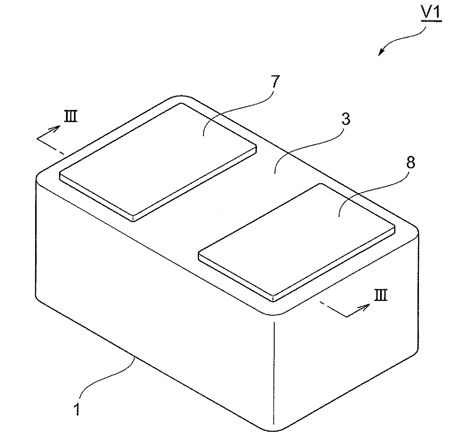
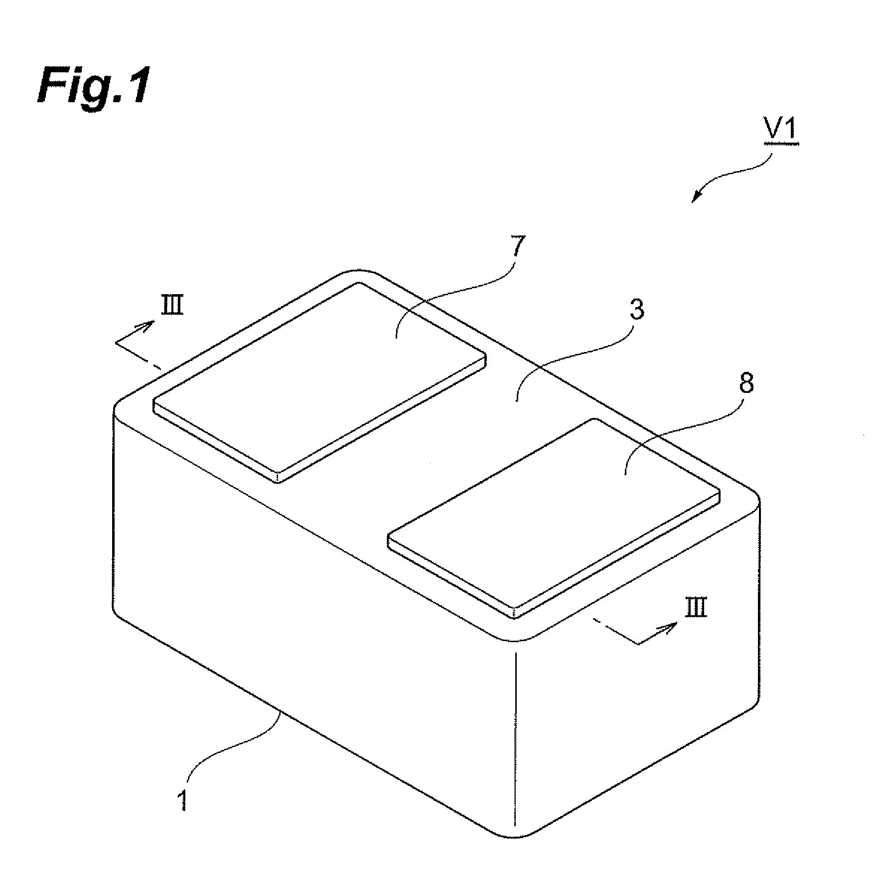
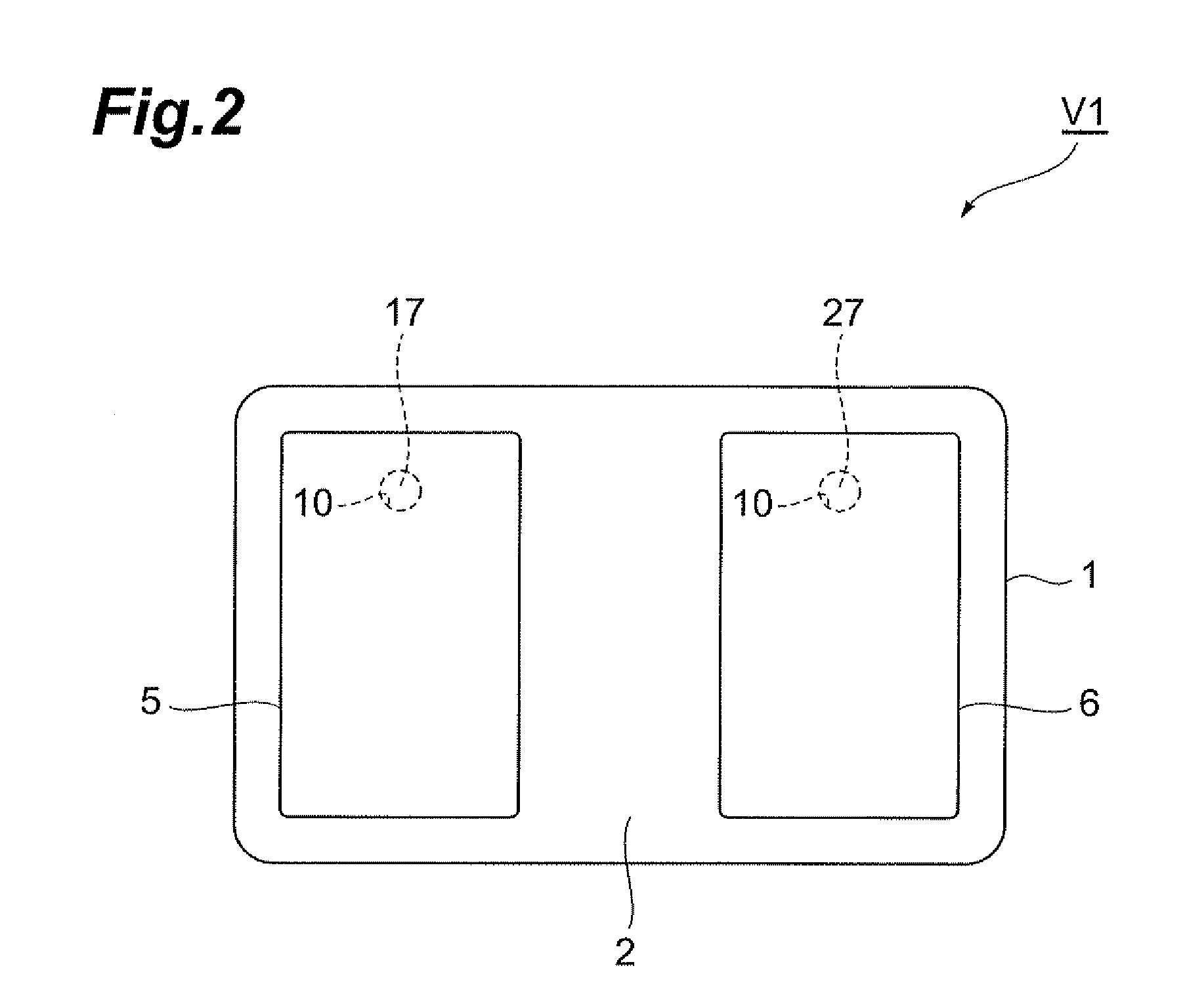
[0025]A configuration of a multilayer chip varistor V1 according to the present embodiment will be described with reference to FIGS. 1 to 4. FIG. 1 is a perspective view showing the multilayer chip varistor V1 of the present embodiment. FIG. 2 is a bottom view showing the multilayer chip varistor V1 of the present embodiment. FIG. 3 is a sectional view along line III-III shown in FIG. 1, of the multilayer chip varistor V1 of the present embodiment. FIG. 4 is a development view where a varistor element body 1 is developed for illustrating each of varistor layers 9. FIG. 3 is depicted without hatching, in order to clearly show configurations of respective components. FIG. 4 is depicted without illus...


PUM


Abstract

A multilayer chip varistor is provided as one capable of suppressing production of cracks and thereby preventing a connection failure between an internal electrode and a through-hole conductor. An internal electrode 21 is so configured as to be curved toward a direction of penetration of a through hole 10 in a connection portion 28 thereof to a through-hole conductor 27. By this configuration, a region T sandwiched between a curved surface 28a of the connection portion 28 and the through-hole conductor 27 is formed in a varistor layer 9 near the connection portion 28. In this region T, a metal concentration thereof becomes higher because of diffusion of metal of the internal electrode 21 and the through-hole conductor 27 into the varistor layer 9, and therefore, after completion of firing, the region T has an intermediate contraction percentage between that of the internal electrode 21 and through-hole conductor 27 and that of the other region of the varistor layer 9. This permits the region T to relax stress near the connection portion 28 where the internal electrode 21, through-hole conductor 27, and varistor layer 9 are congested so as to readily produce cracks.

Description

BACKGROUND OF THE INVENTION[0001]1. Field of the Invention[0002]The present invention relates to a multilayer chip varistor.[0003]2. Related Background Art[0004]There is a known multilayer chip varistor having a varistor layer provided through firing to be integrated on a ceramic insulating substrate, a plurality of internal electrodes provided as opposed to each other with a part of the varistor layer in between, external electrodes provided on the exterior surface of the varistor layer, and through-hole conductors electrically connecting the external electrodes and the plurality of internal electrodes (e.g., cf. Japanese Patent Application Laid-open No. 2006-269876).SUMMARY OF THE INVENTION[0005]For producing the above-described multilayer chip varistor, through holes are formed in ceramic green sheets containing a ceramic powder whose major component is ZnO, and a conductor paste containing a metal (e.g., Ag or the like) as a major component is used to form conductor patterns for...

Claims


Application Information

Patent Timeline
Patent Type & Authority Applications(United States)
IPC IPC(8): H01C7/10
CPCH01C1/142H01C7/18H01C7/1006H01C1/148
Inventor SATO, HIROYUKITAKEUCHI, GOROTAGUCHI, OSAMUTANAKA, RYUICHI
Owner TDK CORPARATION
Why Eureka
Try Eureka