
High density trench field effect transistor

Active Publication Date: 2010-03-18
SEMICON COMPONENTS IND LLC
View PDF16 Cites 32 Cited by
  • Summary
  • Abstract
  • Description
  • Claims
  • Application Information

AI Technical Summary

Benefits of technology

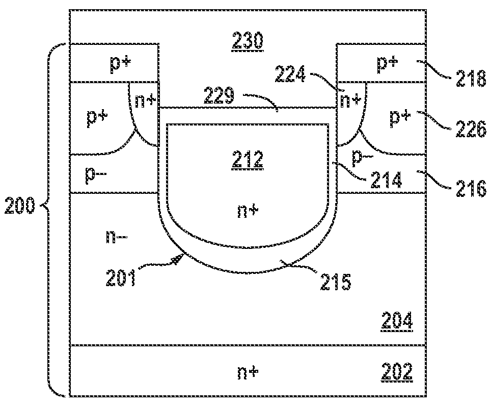
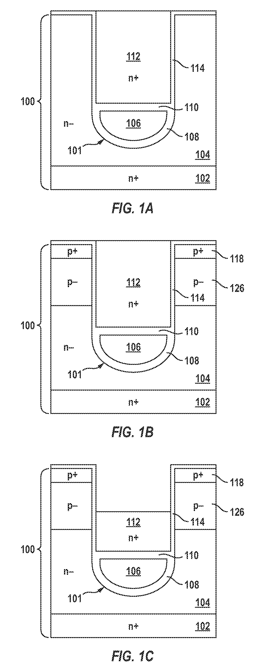
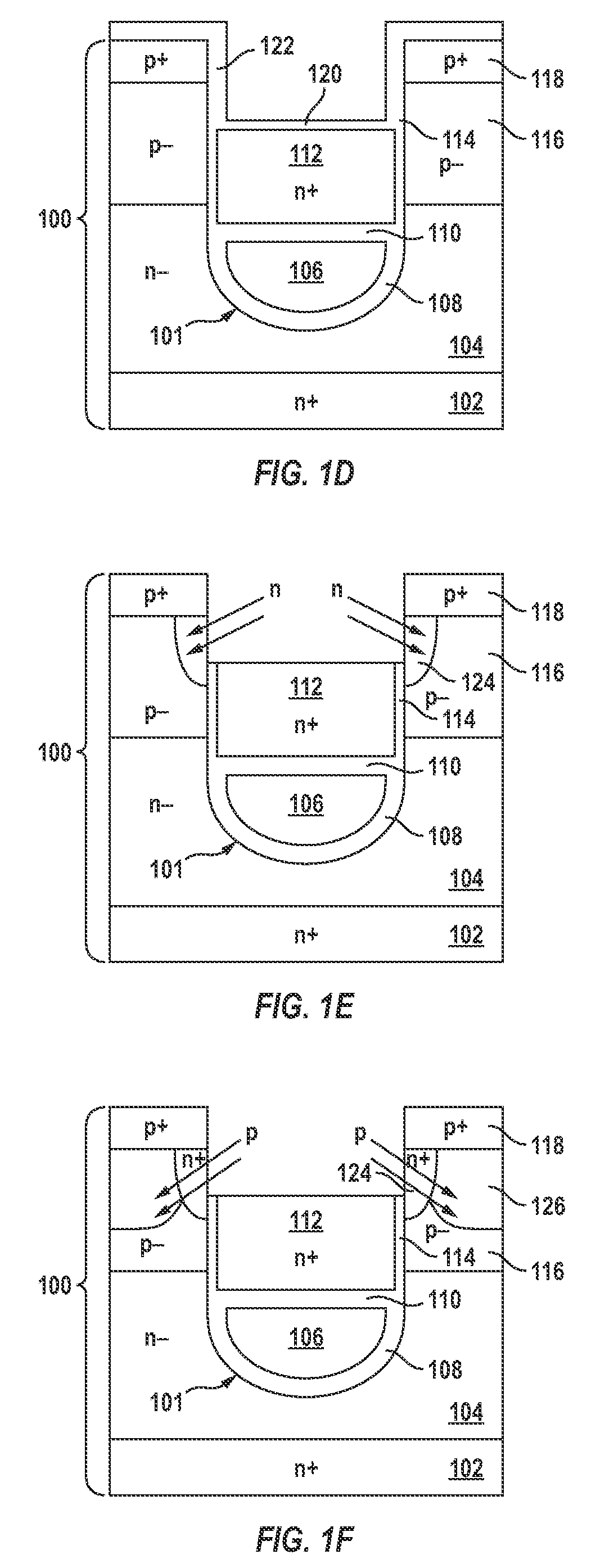
[0009]In accordance with another embodiment of the invention, a trench field effect transistor (FET) is formed as follows. Trenches are formed extending into a semiconductor region. Well regions of a first conductivity type are formed in the semiconductor region. Heavy body regions of the first conductivity type are formed in the well regio

Problems solved by technology

However, both of these dimensions are limited by constraints imposed by manufacturing equipment, structural requirements, alignment tolerances, and transistor operational requirements.
For example, the minimum width of the mesa region between adjacent trenches is limited by the space required for forming source and heavy body regions.
Alignment tolerances associated with forming the trenches and the source and heavy body regions further limit cell pitch reduction.
Many techniques for reducing the cell pitch of trench FETs have been proposed, but none have been able to achieve a substantial reduction in cell pitch without significantly complicating the manufacturing process or adversely impacting transistor performance.

Method used


Image

  • High density trench field effect transistor
  • High density trench field effect transistor
  • High density trench field effect transistor

Examples


Embodiment Construction

[0022]In accordance with embodiments of the present invention, trench FET structures with reduced cell pitch are obtained using simple manufacturing processes. Some embodiments include FET structures with source regions under the heavy body regions. Other embodiments include FET structures with a source region inside the trench. Each of these embodiments allows cell pitch to be reduced by moving the source regions away from the surface of the mesa regions, thus allowing a smaller minimum width of the mesa regions. These and other embodiments of the invention as well as other features and advantages are described in more detail below.

[0023]It should be understood that the following description is exemplary only, and the scope of the invention is not limited to these specific examples. Note that the dimensions in the figures of this application are not to scale, and at times the relative dimensions are exaggerated or reduced in size to more clearly show various structural features. Ad...


PUM


Abstract

A semiconductor structure comprises trenches extending into a semiconductor region. Portions of the semiconductor region extend between adjacent trenches forming mesa regions. A gate electrode is in each trench. Well regions of a first conductivity type extend in the semiconductor region between adjacent trenches. Source regions of a second conductivity type are in the well regions. Heavy body regions of the first conductivity type are in the well regions. The source regions and the heavy body regions are adjacent trench sidewalls, and the heavy body regions extend over the source regions along the trench sidewalls to a top surface of the mesa regions.

Description

BACKGROUND OF THE INVENTION[0001]The present invention relates in general to semiconductor technology, and more particularly, to structures and methods for forming semiconductor devices in shielded and non-shielded gate trench field effect transistors (FETs) with minimum cell pitch.[0002]To increase transistor packing density of trench FETs, it is desirable to minimize the trench width as well as the mesa width (i.e., the spacing between adjacent trenches). However, both of these dimensions are limited by constraints imposed by manufacturing equipment, structural requirements, alignment tolerances, and transistor operational requirements. For example, the minimum width of the mesa region between adjacent trenches is limited by the space required for forming source and heavy body regions. Alignment tolerances associated with forming the trenches and the source and heavy body regions further limit cell pitch reduction.[0003]Many techniques for reducing the cell pitch of trench FETs ha...

Claims


Application Information

Patent Timeline
IPC IPC(8): H01L29/78
CPCH01L21/26586H01L29/0865H01L29/1095H01L29/7813H01L29/66734H01L29/7397H01L29/42368H01L29/42312
Inventor PAN, JAMESHUNT, SCOTT L.PROBST, DEAN E.PARAVI, HOSSEIN
Owner SEMICON COMPONENTS IND LLC
Learn More