
Method for manufacturing a semiconductor component, as well as a semiconductor component, in particular a membrane sensor

Active Publication Date: 2009-05-21
ROBERT BOSCH GMBH
View PDF7 Cites 7 Cited by
  • Summary
  • Abstract
  • Description
  • Claims
  • Application Information

AI Technical Summary

Benefits of technology

[0012]By growing the first epitaxy layer on the stabilizing element, the produced membrane advantageously has greater stability since, first of all, the stabilizing element supports the first epitaxy layer and, secondly, a uniform growing of the first epitaxy layer on the stabilizing element is possible without crystal faults.
[0020]The manufacturing method according to the present invention provides the particular advantage that the rigidity of the membrane may be adjusted via the positioning of the openings on the stabilizing element, and / or that the webs may be designed by varying different manufacturing parameters. The parameters during the epitaxial growth, the geometric arrangement of the openings and / or the lateral or vertical extensions of the webs may be considered manufacturing parameters. For instance, webs having a triangular cross section or having different vertical and / or lateral extensions are able to be produced.
[0022]In an example embodiment of the present invention, a third region, which likewise has the first doping, is produced above the first region, having the first doping, in the semiconductor substrate. The doping of the third region has a higher doping concentration than the doping of the first region. Furthermore, it is provided that, above the first and the third regions, the second epitaxy layer be produced with a second doping that is differentiable from the first doping. By patterning the second epitaxy layer, it is possible to gain access to the third and finally to the first region through the epitaxy layer in a further method step. Afterwards an etching method is utilized to remove the semiconductor material, which method selectively dissolves out only the semiconductor material having the first doping, but will not attack the material having the second doping. By choosing the higher doping concentration in conjunction with an appropriate etching method, more semiconductor material is able to be dissolved out of the third region than is dissolved out of the first region. Such a method makes it possible to produce a virtually planar underside in the stabilizing element formed in this manner.

Problems solved by technology

These surface micromechanical methods are comparatively costly, on account of the necessity for separate sacrificial layers.
However, tests have shown that at least partially porous membrane may get damaged during manufacture, or that damage may not always be reliably prevented under normal operating conditions.

Method used


Image

  • Method for manufacturing a semiconductor component, as well as a semiconductor component, in particular a membrane sensor
  • Method for manufacturing a semiconductor component, as well as a semiconductor component, in particular a membrane sensor
  • Method for manufacturing a semiconductor component, as well as a semiconductor component, in particular a membrane sensor

Examples


Embodiment Construction

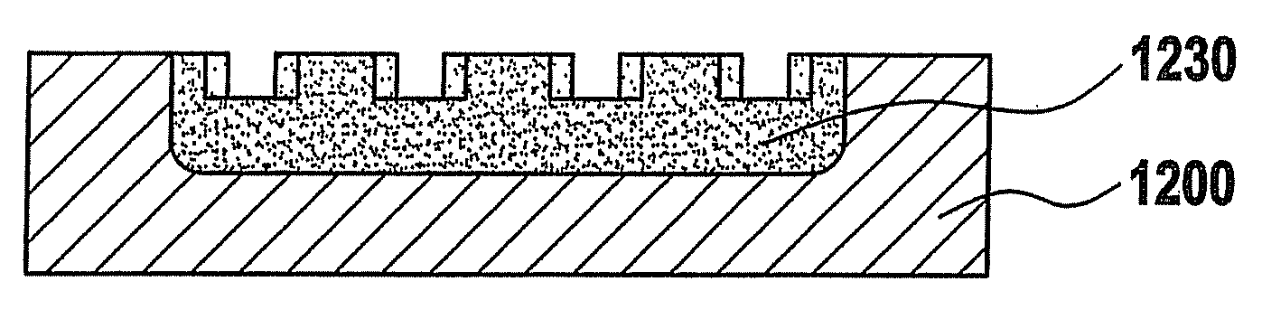
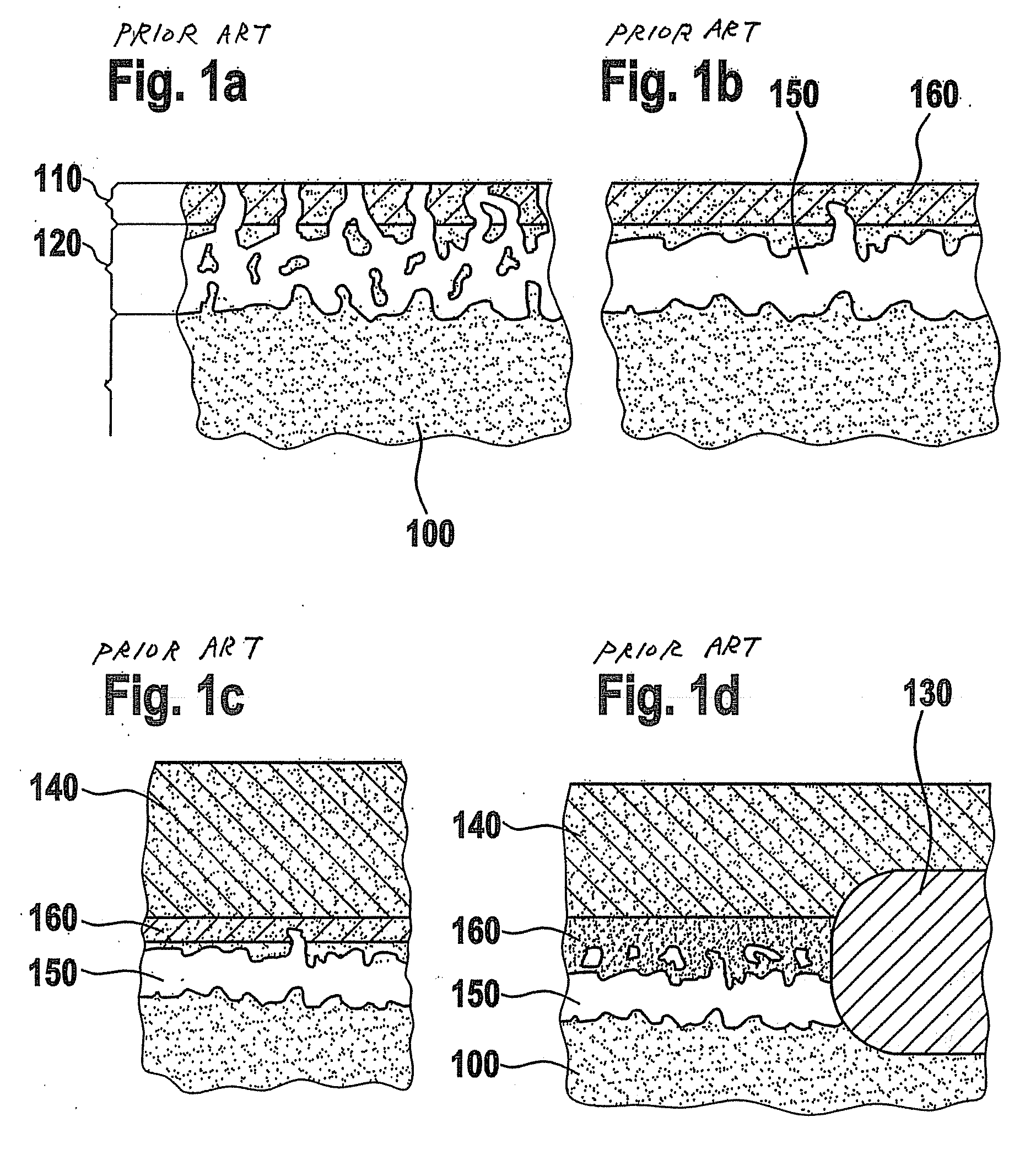
[0043]As shown in FIG. 1a, a conventional method for producing a membrane provides using a porous double layer in a semiconductor substrate 100, i.e., using a low-porosity layer 110 and a high-porosity layer 120 situated underneath it, it is possible to produce a starting layer 160 that is suitable for the growth of epitaxy layer 140, as well as a cavity 150 (cf. FIG. 1b). The transformation is accomplished by a first annealing step (at approximately 900 to 1000° C.), during which the semiconductor atoms of low-porosity layer 110 relocate in such a way that the surface seals. In the same or in a following annealing step, cavity 150 is then able to be formed as well by relocation of the semiconductor atoms out of high-porosity layer 120. This is accomplished in that the pores enlarge under the influence of the annealing step and finally unite to form a “giant pore,” which then constitutes the cavity. An epitaxy layer 140 may then be deposited on starting layer 160 to produce the memb...


PUM


Abstract

A manufacturing method for a micromechanical semiconductor element includes providing on a semiconductor substrate a patterned stabilizing element having at least one opening. The opening is arranged such that it allows access to a first region in the semiconductor substrate, the first region having a first doping. Furthermore, a selective removal of at least a portion of the semiconductor material having the first doping out of the first region of the semiconductor substrate is provided. In addition, a membrane is produced above the first region using a first epitaxy layer applied on the stabilizing element. In a further method step, at least a portion of the first region is used to produce a cavity underneath the stabilizing element. In this manner, the present invention provides for the production of the patterned stabilizing element by means of a second epitaxy layer, which is applied on the semiconductor substrate.

Description

CROSS-REFERENCE TO RELATED APPLICATION[0001]This application is a divisional of, and incorporates herein by reference in its entirety, U.S. patent application Ser. No. 11 / 011,888, which was filed on Dec. 13, 2004 and which claims priority under 35 U.S.C. § 119 of German Patent Application No. DE 103 58 859.0 filed on Dec. 16, 2003 and German Patent Application No. 10 2004 036 032.4 filed on Jul. 24, 2004.FIELD OF THE INVENTION[0002]The present invention relates to a method for manufacturing a semiconductor component.BACKGROUND INFORMATION[0003]Semiconductor elements, and membrane sensors, in particular, as well as methods for producing membrane sensors on the base of semiconductor substrates such as silicon wafers are already known. For instance, flat porous membrane regions are arranged on the semiconductor substrate as substrate for sensor structures, and a cavity is produced underneath the membrane, e.g., for the thermal insulation of the membrane.[0004]The membrane sensors curre...

Claims


Application Information

Patent Timeline
IPC IPC(8): H01L29/84H01L21/3213B81B3/00B81C1/00G01L9/00H01L21/00H01L29/24H01L33/00
CPCB81B3/007B81B2201/0264B81B2203/0127B81C2201/0136B81C2201/0115B81C2201/0116B81C1/00658
Inventor BENZEL, HUBERTSCHAEFER, FRANKARMBRUSTER, SIMONLAMMEL, GERHARDSCHELLING, CHRISTOPHBRASAS, JOERG
Owner ROBERT BOSCH GMBH
Learn More