System and method for improving the efficiency and reliability of a broadband transistor switch for periodic switching applications

a broadband transistor and periodic switching technology, applied in electronic switching, oscillator generators, pulse techniques, etc., can solve the problems of difficult supply of direct current (dc) power for operation, voltage loss, etc., to optimize switching performance, and reduce the cost of operation.

Inactive Publication Date: 2010-04-01
UNITED STATES OF AMERICA
View PDF9 Cites 6 Cited by
  • Summary
  • Abstract
  • Description
  • Claims
  • Application Information

AI Technical Summary

Benefits of technology

[0015]The concept is that an ideal switch can be used to efficiently convert a DC power source to a square-wave and that an ideal diode can be used to convert a square-wave source to DC. A nearly ideal switch can be emulated by the collector-emitter path of a transistor. Recognizing that the base-emitter junction is a diode, allows the basic concept to be employed to convert the transistor to be employed to convert the transistor into a nearly ideal switch.
[0016]This concept allows precision control of the base-emitter current in the “ON” state of the switch and allows precision control of the base-emitter reverse bias in the “OFF” state of the switch. If the “ON” state base-emitter current is too large, excess charge is stored in the transistor, which slows the switching process when the transistor is switched from “ON” to “OFF”. If the base-emitter reverse bias is too large in the “OFF” state, the transistor may fail catastrophically. Thus the use of the basic concept is to provide precision control of the transistor switching parameters which is essential to the operation of the transistor as an efficient switch. Furthermore, the present invention protects the switching transistor and optimizes switching performance by permitting independent and precise control of a transistor base current and base-emitter-junction reverse-bias voltage.
[0018]The disclosure describes a method for using a transistor as a periodic switch with low “ON” state resistance and high “OFF” state resistance. When a transistor is used as a switch, it is necessary to precisely control the base-emitter current so that, in the ON state, excess charge is stored in the base-emitter junction is minimized and it is also necessary, in the OFF state to precisely control the base-emitter reverse bias voltage. If excess charge is stored in the base-emitter junction, switching latency is increased. If the base emitter reverse bias limits are exceeded, the transistor may be destroyed. The method of this disclosure permits precision control of the ON state base-emitter current and of the OFF state base-emitter reverse bias in order to optimize the performance of the transistor as a switch and preserve the life time of the transistor in this application.
[0022]The transistor switch may be configured for use in 1) a single-ended, or shunt mode or in 2) a balanced, or series mode. The method disclosed herein supports the shunt mode and the series mode of operation. A shunt-mode switch is usually configured using only one PNP or NPN transistor with emitter connected to the circuit common ground. A series mode switch is usually configured with one PNP and one NPN transistor connected emitter-to-emitter so that the base-emitter current of the PNP transistor is the same as the emitter-base current of the NPN transistor. The base-emitter-emitter-base connection appears as two diodes connected in series and acting as a single diode. The method of this application can then be used to drive this single diode and to create a balanced square-wave drive that can be passed through a transformer because there is no average DC current required to drive the series switch. Thus, the method described herein allows the use of a transformer to absorb the common-mode voltage of the circuit allowing the series switch to appear to float in the switching application.
[0024]A novel feature of the disclosed circuit design is that the combination of circuit elements comprising the base-emitter drive circuit presents a matched termination to a square wave. Thus the length of the transmission line that connects the base-emitter drive circuit to a square-wave source will not affect the switching characteristics of the periodic transistor switch. The practical importance of the matched condition is that the primary source of the square wave drive may be located a significant distance from the location of the transistor switch. In one embodiment, the transistor switch may be located adjacent to an antenna so that the maximum RF power generated by the periodic switching action will be radiated while the modulation source is located in a protected shelter and connected to the high-power transistor switch by means of a transmission line. If the transmission line were mismatched, then standing waves on the transmission line would affect the switching properties, which would in turn limit the frequency band of operation.

Problems solved by technology

Direct Current (DC) power for operation is difficult to supply because of the long length and / or the small size of the sensor tethers.
The driven device input has a capacitance associated therewith, which normally results in a voltage loss as this capacitance is alternately charged and discharged.

Method used


Image

  • System and method for improving the efficiency and reliability of a broadband transistor switch for periodic switching applications
  • System and method for improving the efficiency and reliability of a broadband transistor switch for periodic switching applications
  • System and method for improving the efficiency and reliability of a broadband transistor switch for periodic switching applications

Examples


Embodiment Construction

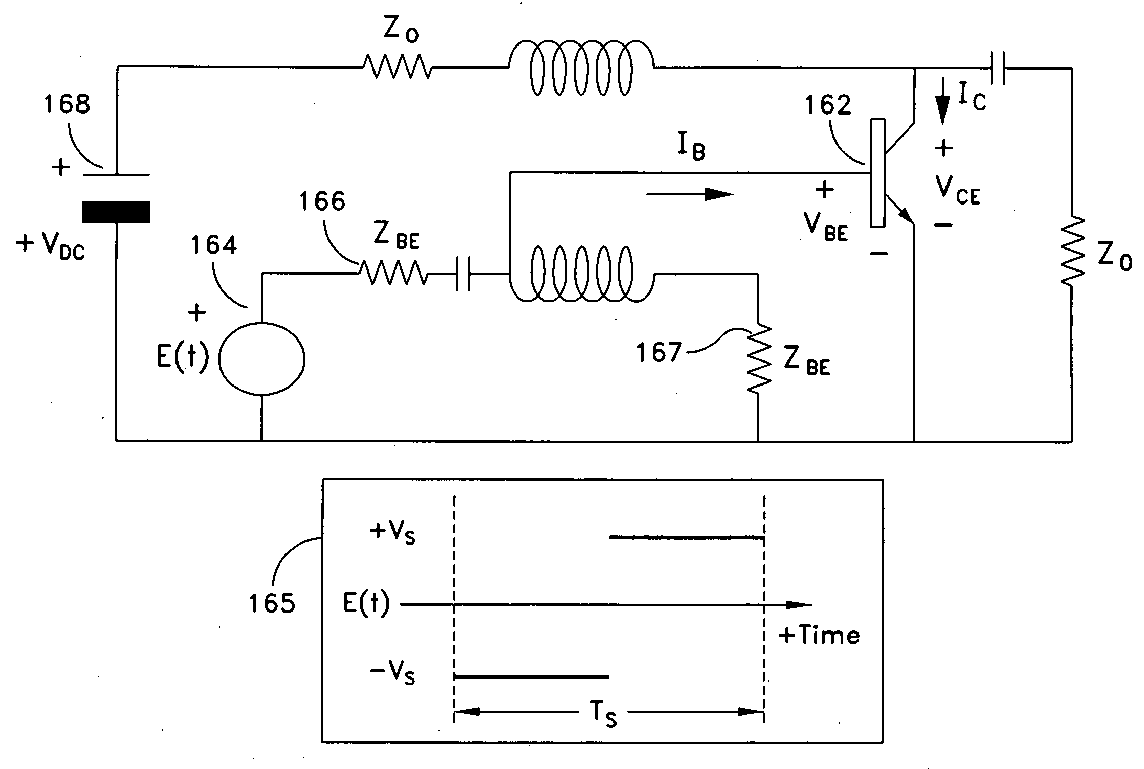
[0046]The description of a switch driver design is presented in five sections. In a first section, concepts are introduced that explain circuit operation in the following sections. In a second section, the operation of an energy efficient square-wave generator is disclosed. The square-wave generator circuit provides a foundation for the amplitude-phase modulator design disclosed in a fifth section. In a third section, an energy efficient [square-wave]-to-DC converter is disclosed, which provides a foundation for the switch driver design disclosed in a fourth section.

Introduction to the Disclosed Method

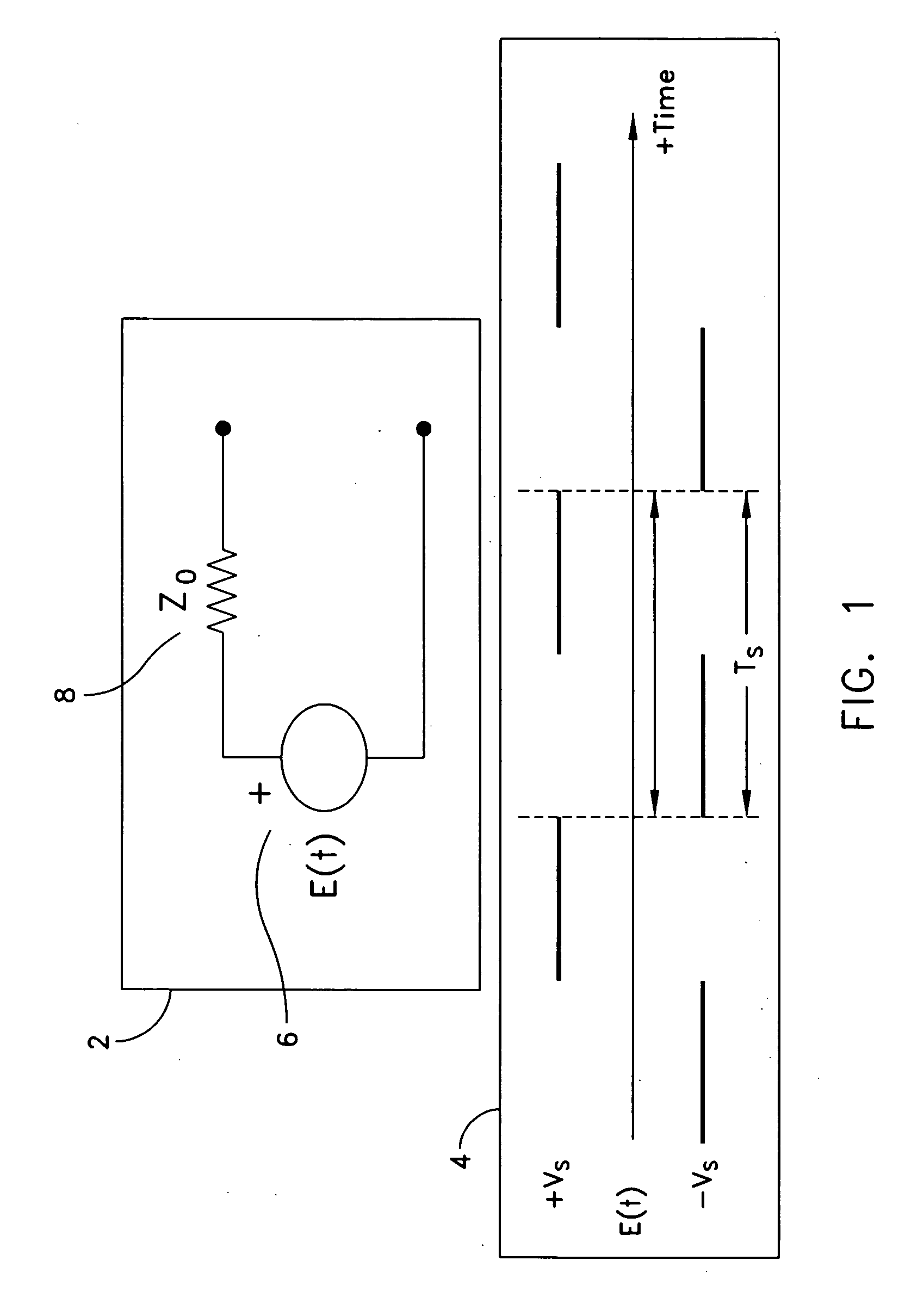
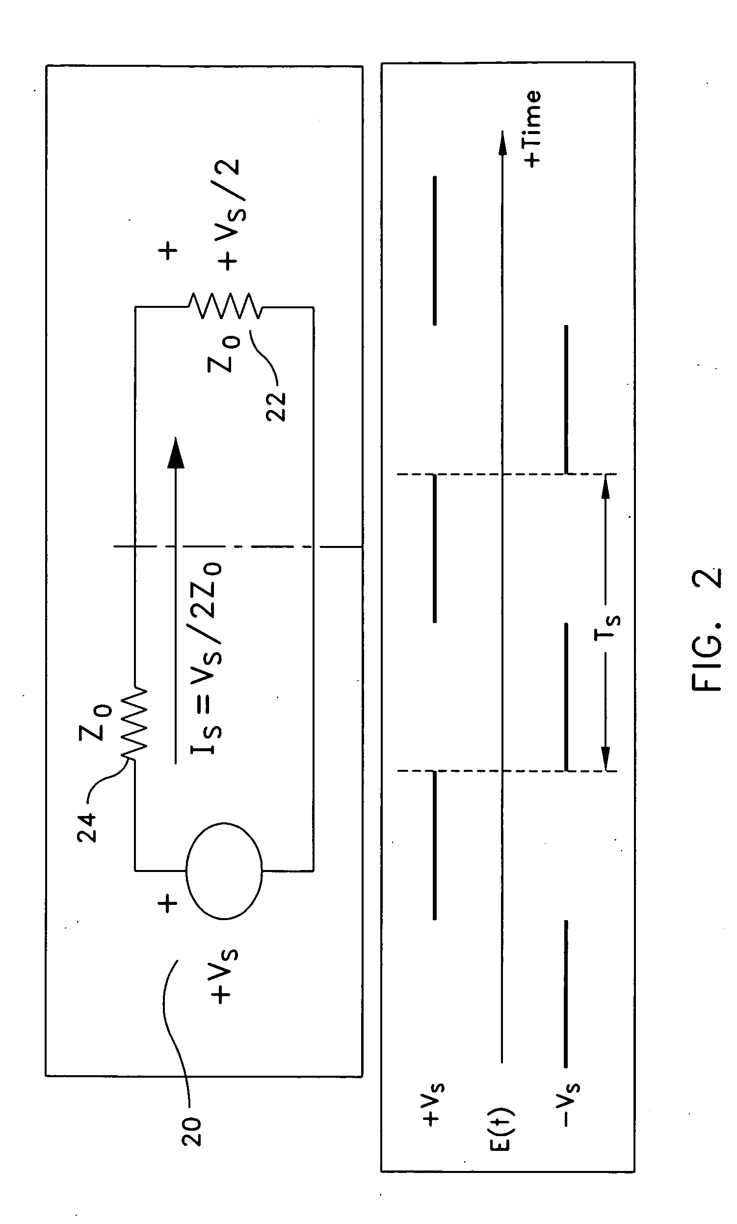
[0047]In FIG. 1, a Thevenin-Equivalent source 2 is shown. A voltage 4 of a signal generator 6 switches between a positive state, +VS and a negative state, −VS, in which the states have the same magnitude but opposite polarity. The switching operation is periodic with a period, TS, and with equal dwell times in each state. Thus, the average value of the generator voltage is zero. Furthe...


PUM


Abstract

A driver circuit is provided for enabling a transistor collector-emitter path to be used as a broadband periodic switch. The broadband driver circuit controls the magnitude of the transistor base-emitter current in order to enable a CLOSED switch state and to simultaneously control the magnitude of the transistor base-emitter reverse-bias voltage in order to enable the OPEN-switch state. The precise control of these parameters minimizes base-charge storage and prevents reverse-breakdown failure.

Description

CROSS-REFERENCE TO RELATED APPLICATIONS[0001]The application submitted herein is related to: U.S. patent application Ser. No. 12 / 022,506, filed on Jan. 30, 2008 entitled “A Method for Coupling a Direct Current Power Source Across a Dielectric Membrane or Other Non-Conducting Membrane” and U.S. patent application Ser. No. 12 / 022,537 filed on Jan. 30, 2008 entitled “A Method for Coupling a Direct Current Power Source Across a Nearly Frictionless High-Speed Rotation Boundary”. Both applications are by the inventor, Dr. Donald H. Steinbrecher.STATEMENT OF GOVERNMENT INTEREST[0002]The invention described herein may be manufactured and used by or for the Government of the United States of America for governmental purposes without the payment of any royalties thereon or therefor.BACKGROUND OF THE INVENTION[0003](1) Field of the Invention[0004]The present invention relates to a system and method of use for a broadband transistor switch in periodic switching applications.[0005](2) Descriptio...

Claims


Application Information

Patent Timeline
Patent Type & Authority Applications(United States)
IPC IPC(8): H03K17/60
CPCH03K17/601
Inventor STEINBRECHER, DONALD H.
Owner UNITED STATES OF AMERICA
Why Eureka
Try Eureka