Interconnect Structures and Methods

a technology of interconnection and structure, applied in the direction of semiconductor devices, semiconductor/solid-state device details, electrical devices, etc., can solve problems such as misalignment between dies

Inactive Publication Date: 2010-04-15
POLARIS INNOVATIONS LTD
View PDF3 Cites 42 Cited by
  • Summary
  • Abstract
  • Description
  • Claims
  • Application Information

AI Technical Summary

Problems solved by technology

However, alignment marks and alignment procedures are required to align the two die using this method, which requires additional manufacturing and processing steps and may result in misalignment between the die.

Method used


Image

  • Interconnect Structures and Methods
  • Interconnect Structures and Methods
  • Interconnect Structures and Methods

Examples


Embodiment Construction

[0014]The making and using of the presently preferred embodiments are discussed in detail below. It should be appreciated, however, that the present invention provides many applicable inventive concepts that can be embodied in a wide variety of specific contexts. The specific embodiments discussed are merely illustrative of specific ways to make and use the invention, and do not limit the scope of the invention.

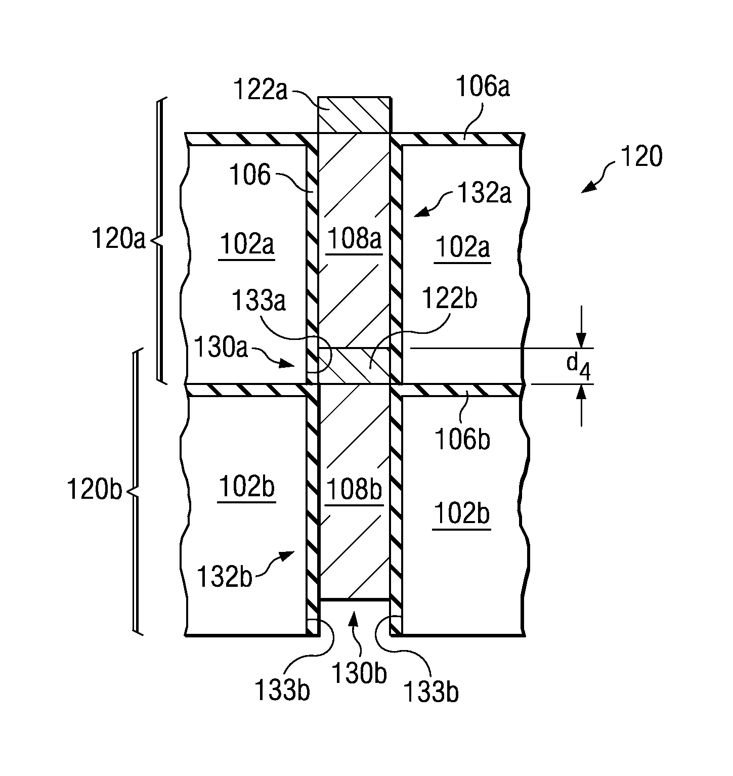
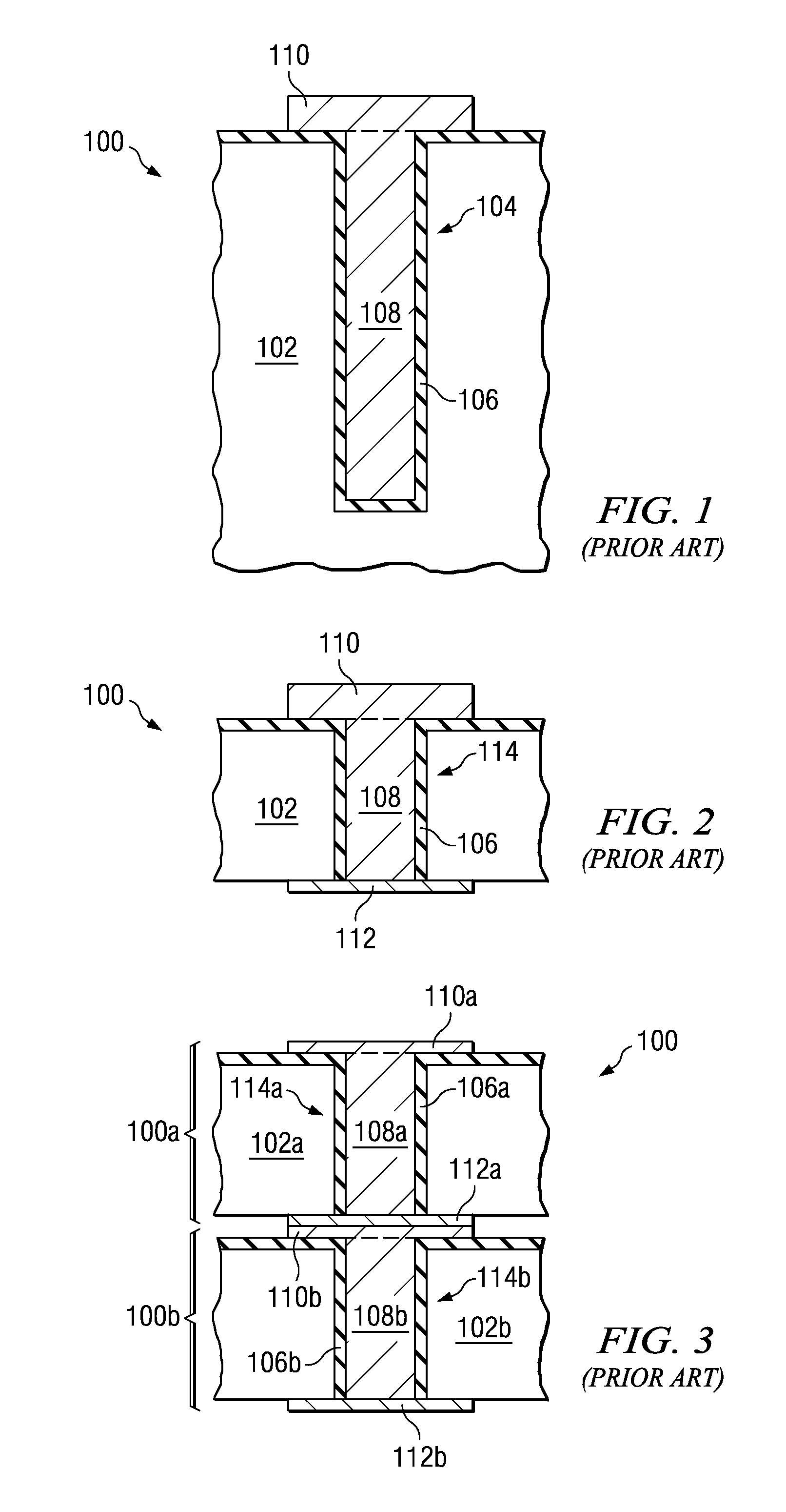
[0015]FIGS. 1 through 3 show cross-sectional views of a prior art method of connecting together two semiconductor die or devices 100 using through-silicon vias 114a. FIG. 1 shows a workpiece 102 comprising a semiconductor wafer that comprises a semiconductor material such as silicon. Through-silicon vias 114a are formed by etching a via 104 partially through the workpiece 102, e.g., using lithography. An insulating material layer 106 comprising an insulator is formed over the workpiece 102, lining the via 104. A conductive material 108 is deposited over the workpiece 102, fil...


PUM


Abstract

Interconnect structures and methods are disclosed. In one embodiment, an interconnect structure includes a via extendable through a workpiece from a first side of the workpiece to a second side of the workpiece. The via is partially filled with a conductive material and has sidewalls. The interconnect structure includes a contact coupled to the conductive material in the via proximate the first side of the workpiece. The conductive material in the via comprises a recessed region comprising a landing zone proximate the second side of the workpiece.

Description

TECHNICAL FIELD[0001]The present invention relates generally to semiconductor devices, and more particularly to interconnect structures and methods.BACKGROUND[0002]Semiconductor devices are used in a variety of electronic applications, such as personal computers, cell phones, digital cameras, and other electronic equipment, as examples. Semiconductor devices are typically fabricated by sequentially depositing insulating or dielectric layers, conductive layers, and semiconductive layers of material over a semiconductor substrate, and patterning the various layers using lithography to form circuit components and elements thereon.[0003]Semiconductor devices are typically packaged as single die or in multi-chip modules. Many different types of packaging are used, and packaging techniques have changed throughout the years as semiconductor devices are scaled down in size and according to the end application. Factors such as performance, size, weight, and operating conductions influence th...

Claims


Application Information

Patent Timeline
Patent Type & Authority Applications(United States)
IPC IPC(8): H01L23/52H01L21/44
CPCH01L21/76898H01L23/481H01L25/0657H01L25/50H01L2224/81141H01L2225/06541H01L2224/16147H01L2224/16237H01L2224/81191H01L2225/06513H01L2224/05009H01L2224/0557H01L2224/05568H01L2224/05001H01L2224/051H01L2224/05647H01L2224/16146H01L24/16H01L24/13H01L24/05H01L2224/0401H01L2224/131H01L2224/13025H01L2924/00014H01L2924/013H01L2924/014
Inventor ZIMMERMANN, BERNDBERGHOF, VOLKERRUCKMICH, STEFANSCHEDEL, THORSTEN
Owner POLARIS INNOVATIONS LTD
Why Eureka
Try Eureka