Strip line filter

a filter and strip line technology, applied in the direction of waveguides, basic electric elements, waveguide type devices, etc., can solve the problems of low accuracy, difficult to reduce the width of gaps between input/output electrodes and ground electrodes, and low production cost, so as to enhance the degree of freedom of arrangement of top-surface lines connected to side-surface lines

Inactive Publication Date: 2010-04-15
MURATA MFG CO LTD
View PDF8 Cites 0 Cited by
  • Summary
  • Abstract
  • Description
  • Claims
  • Application Information

AI Technical Summary

Benefits of technology

[0016]According to the preferred embodiments of the present invention, since the terminal portions of the side-surface lines near the top surface and the corresponding terminal portions of the side-surface lines near the bottom surface are deviated from each other, a degree of freedom of arrangement of the top-surface lines connected to the side-surface lines is enhanced. Accordingly, gap widths between the input / output electrodes and the ground electrode and sizes of the input / output electrodes are ensured while the top-surface lines are arranged so as to attain required filter characteristics. Consequently, a small filter having the required filter characteristic is realized while restriction of arrangement of an electrode pattern on a bottom surface of a dielectric substrate is satisfied.

Problems solved by technology

In this case, however, in terms of production cost, a low-accuracy coating process is generally used for formation of electrode patterns on side surfaces and a bottom surface.
Although size reduction of electrode patterns has been required for size reduction of a chip in recent years, since accuracy of electrode patterns on side surfaces and a bottom surface is low, it is difficult to reduce widths of gaps between input / output electrodes and a ground electrode and to reduce sizes of the input / output electrodes.
Therefore, arrangement of the electrode pattern on the top surface is also restricted, and consequently, it may be difficult to attain required filter characteristics.

Method used


Image

  • Strip line filter
  • Strip line filter
  • Strip line filter

Examples


first embodiment

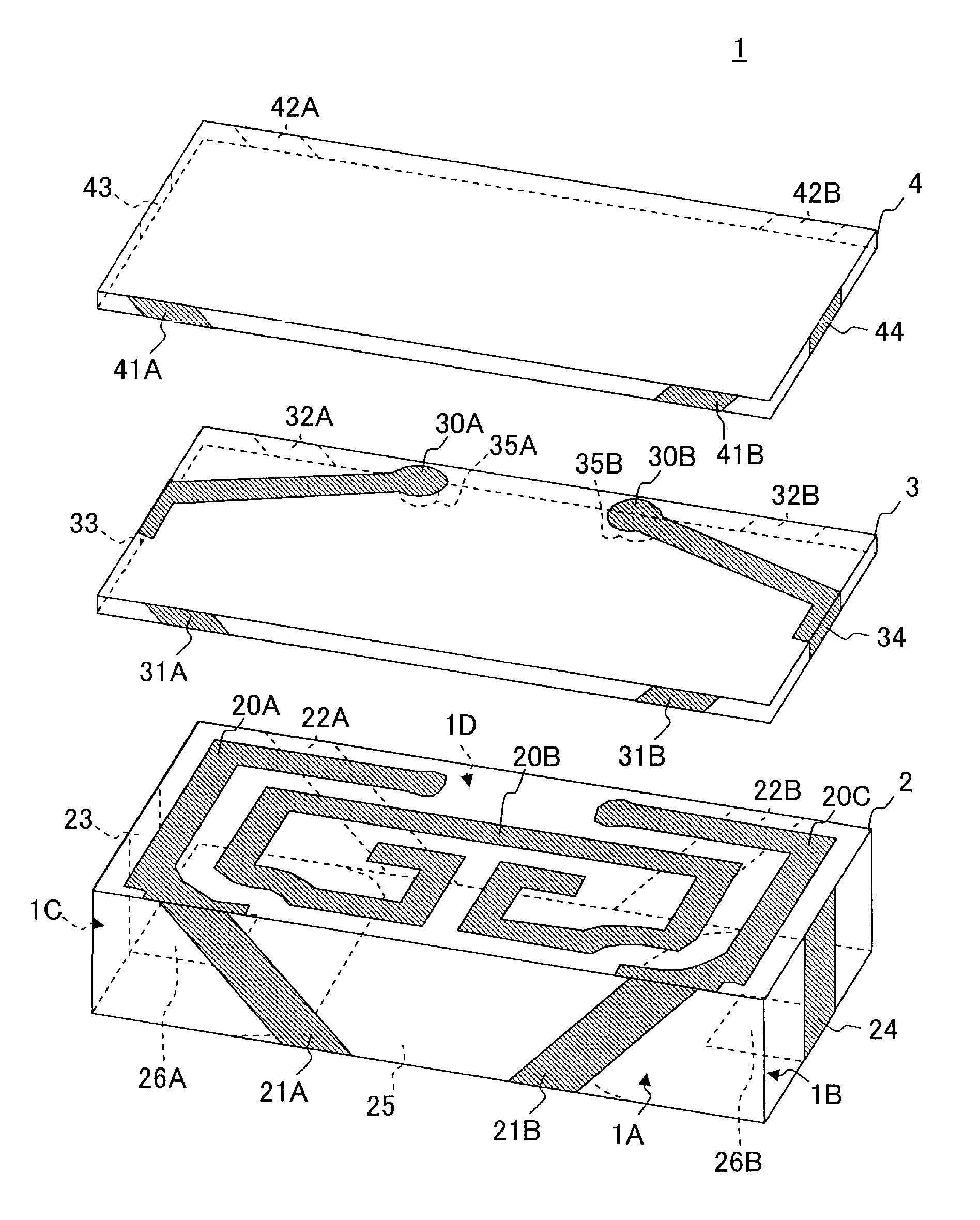
[0025]A strip line filter 1 according to the present invention will now be described.

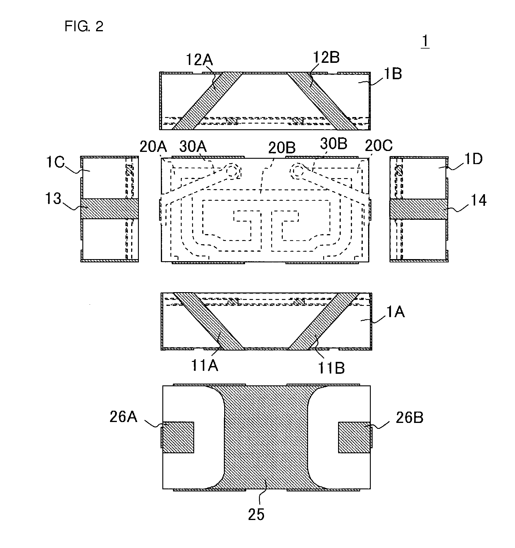
[0026]The strip line filter 1 of this embodiment is a band pass filter for high bands of UWB (Ultra Wide Band) communication. FIG. 2 is a development view illustrating the strip line filter 1 of this embodiment.

[0027]The strip line filter 1 includes side-surface lines 11A and 11B on a front surface 1A thereof. On a back surface 1B of the strip line filter 1, side-surface lines 12A and 12B are arranged. On a left surface 1C, a side-surface line 13 is arranged. On a right surface 1D, a side-surface line 14 is arranged. On a bottom surface serving as an implementing surface, a ground electrode 25 and input / output electrodes 26A and 26B are arranged. The ground electrode 25 and the input / output electrodes 26A and 26B are arranged separately from each other. When the strip line filter 1 is implemented on an implementing substrate, high-frequency-signal input / output terminals are connected to the input / ou...

second embodiment

[0044]Next, a strip line filter 50 according to the present invention will be described.

[0045]FIG. 4 is a development view illustrating the strip line filter 50 of this embodiment. The strip line filter 50 has electrode patterns on a front surface 1A and a back surface 1B which are different from those of the first embodiment. Note that components the same as those shown in the first embodiment are denoted by reference numerals the same as those used in the first embodiment and descriptions thereof are omitted.

[0046]On each of the front surface 1A and the back surface 1B of the strip line filter 50, side-surface electrodes 51 are arranged. Each of the side-surface electrodes 51 is formed in a substantially X-shape and has four leg portions 52A, 52B, 52C, and 52D.

[0047]In each of the side-surface electrodes 51, the leg portion 52A is arranged near a bottom surface of a dielectric substrate 2 and arranged on an outer side relative to the center of a corresponding one of the front surf...

third embodiment

[0050]A strip line filter 60 according to the preset invention will now be described.

[0051]FIG. 5 is a development view illustrating the strip line filter 60 of this embodiment. The strip line filter 60 has electrode patterns on a front surface 1A and a back surface 1B which are different from those of the first and second embodiments. Note that components the same as those shown in the first embodiment are denoted by reference numerals the same as those used in the first embodiment and descriptions thereof are omitted.

[0052]On each of the front surface 1A and the back surface 1B of the strip line filter 60, side-surface electrodes 61 are arranged. Each of the side-surface electrodes 61 is formed in a substantially H-shape and has four leg portions 62A, 62B, 62C, and 62D and a connection portion 63. In each of the side-surface electrodes 61, the leg portion 62A is arranged near the bottom surface of a dielectric substrate 2 and arranged on an outer side relative to the center of a c...


PUM


Abstract

A strip line filter includes a dielectric substrate having a ground electrode, input/output electrodes, upper-surface lines, and side-surface lines. Certain side-surface lines are connected to the ground electrode at first terminal portions thereof which are positioned near the a bottom surface of the dielectric substrate, and are connected to certain upper-surface lines among the upper-surface lines at second terminal portions thereof which are positioned near a top surface. The second terminal portions of the side-surface lines are deviated from the first terminal portions of the side-surface lines in a direction parallel to the top and bottom surfaces of the dielectric substrate.

Description

BACKGROUND OF THE INVENTION[0001]1. Field of the Invention[0002]The present invention relates to a strip line filter including a dielectric substrate and strip lines arranged on the dielectric substrate.[0003]2. Description of the Related Art[0004]Microstrip line filters including strip-line resonators arranged on dielectric substrates have been used in various fields (refer to Japanese Patent 3018214).[0005]An example of a configuration of a conventional microstrip line filter 100 will be described hereinafter. FIG. 1A is a bottom view illustrating a conventional microstrip line filter according to Japanese Patent 3018214. FIG. 1B is a perspective top view illustrating the microstrip line filter 100.[0006]The microstrip line filter 100 includes a dielectric substrate 101 and another dielectric substrate (not shown) laminated on the dielectric substrate 101. On a bottom surface 101A of the dielectric substrate 101, a ground electrode 104A and input / output electrodes 102A, 102B, 103A...

Claims


Application Information

Patent Timeline
Patent Type & Authority Applications(United States)
IPC IPC(8): H01P1/203
CPCH01P1/20381
Inventor NAKAMURA, SOICHI
Owner MURATA MFG CO LTD
Why Eureka
Try Eureka