Imaging lens, imaging device, portable terminal, and method for manufacturing imaging lens

a technology of imaging lens and portable terminal, which is applied in the direction of mountings, instruments, nanotechnology, etc., can solve the problems that imaging lenses cannot be easily compatible with further size reduction, and achieve the effects of easy production and assembly of imaging lenses, positive optical power, and low cos

Inactive Publication Date: 2010-04-15
KONICA MINOLTA OPTO
View PDF1 Cites 27 Cited by
  • Summary
  • Abstract
  • Description
  • Claims
  • Application Information

AI Technical Summary

Benefits of technology

[0057]According to the present invention, an imaging lens includes one or two lens blocks so as to be compact. In particular, a lens block disposed at the most object-side position exerts a positive optical power, and owing to the difference between the index of refraction of a lens substrate and the index of refraction of a lens L[LS1o] in that lens block, the chromatic aberration in the imaging lens is corrected properly. In addition, fabricating a large number of lenses simultaneously on a single plane-parallel plate makes production and assembly of the imaging lens easy, with the result that the imaging lens is manufactured inexpensively.

Problems solved by technology

Inconveniently, however, these imaging lenses do not promise easy compatibility between further size reduction and higher mass-producibility due to technical limitations.

Method used


Image

  • Imaging lens, imaging device, portable terminal, and method for manufacturing imaging lens
  • Imaging lens, imaging device, portable terminal, and method for manufacturing imaging lens
  • Imaging lens, imaging device, portable terminal, and method for manufacturing imaging lens

Examples


embodiment 1

[0115][▪ Imaging Device and Portable Terminal]

[0116]Typically, imaging lenses are suitably used in digital appliances (for example, portable terminals) equipped with an image capturing capability. This is because a digital appliance including a combination of an imaging lens, an image sensor, etc. functions as an imaging device that optically takes in an image of a subject and outputs it in the form of an electrical signal.

[0117]An imaging device is a main component (optical device) of a camera that shoots still and moving images of a subject, and includes, for example, from the object (i.e. subject) side thereof, an imaging lens that forms an optical image of an object and an image sensor that converts the optical image formed by the imaging lens into an electrical signal.

[0118]Examples of cameras include digital cameras, video cameras, monitoring cameras, vehicle-mounted cameras, and videophone cameras. Cameras may also be incorporated in, or externally fitted to, personal compute...

example 1

[0236]

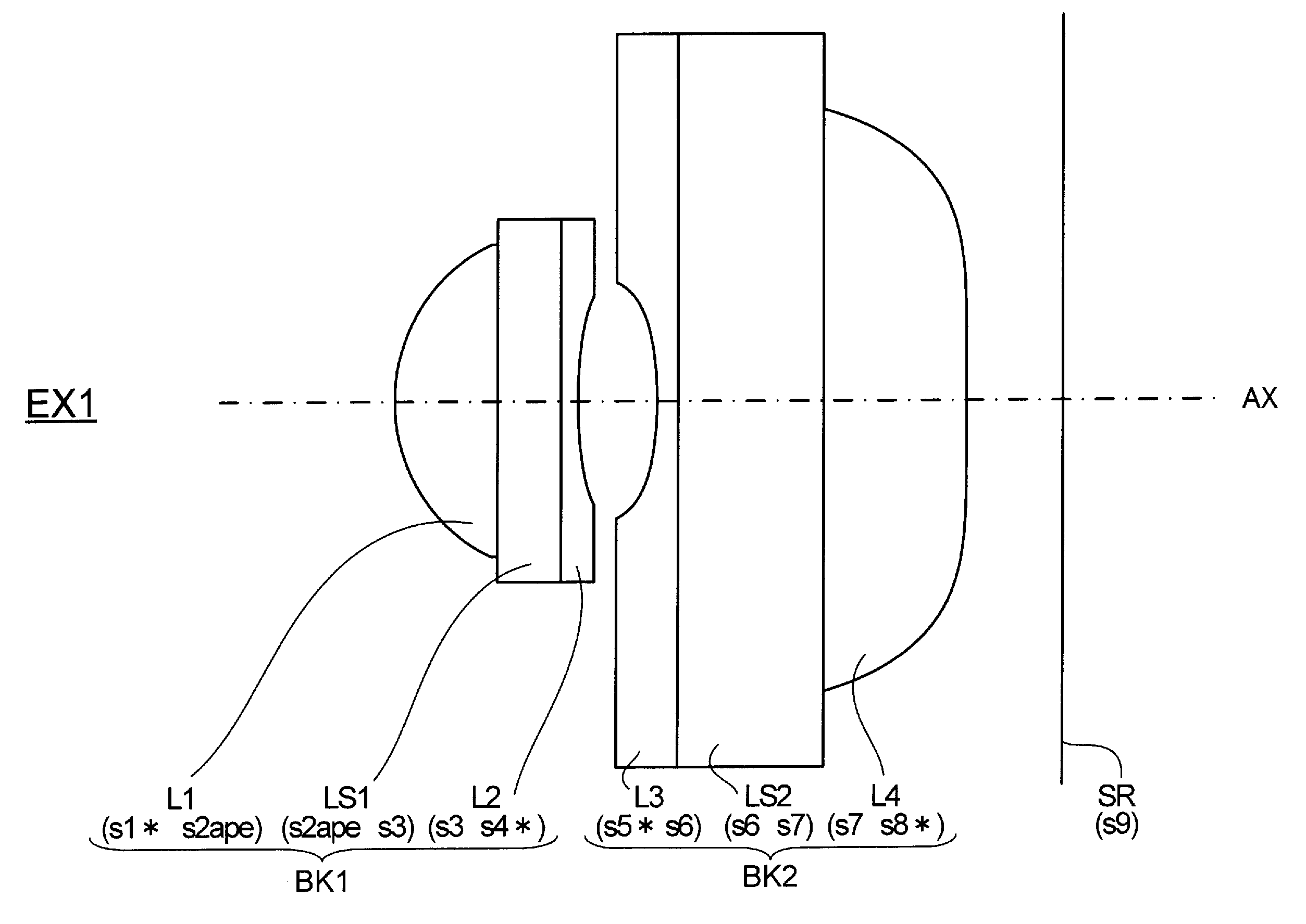
TABLE 1EXAMPLE 1f [mm] 2.964Fno 2.8BF [mm] 0.4625Y′ [mm] 1.750ω [°] 30.56TL [mm] 3.179siir [mm]id [mm]iNdνdElements1*1 0.808L1BK110.48911.507154.00s2ape2∞20.30021.649229.92LS1s33∞30.08031.573729.00L2s4*4 2.30140.373s5*5−1.948L3BK250.10041.507154.00s66∞60.69551.649229.92LS2s77∞70.68061.507154.00L4s8*818.78380.463s99∞SR

TABLE 2EXAMPLE 1Aspherical Surface Datasis1s4s5s8K−1.20E−011.63E+011.04E+01−3.60E+04A1.30E−023.20E−02−4.11E−01−3.72E−02B2.66E−022.71E−013.07E−01−1.36E−01C1.51E−01−9.96E−01−4.63E+005.58E−02D−1.54E−011.63E+009.15E+002.95E−03E−2.05E−01−2.38E+00−4.59E+00−1.45E−02F2.63E+007.12E+01−7.14E+01−4.84E−03G−3.72E+00−3.52E+00−2.51E+014.32E−03H3.33E+00−4.13E+01−6.52E+012.28E−03I2.59E+00−5.28E+02−1.88E+02−1.37E−03

example 2

[0237]

TABLE 3EXAMPLE 2f [mm] 2.979Fno 2.8BF [mm] 0.7526Y′ [mm] 1.750ω [°] 30.43TL [mm] 3.448siir [mm]id [mm]iNdνdElements1*10.934L1BK110.36211.487570.45s2ape2∞20.42721.688647.43LS1s33∞30.07431.688931.16L2s4*42.19440.726L3BK2s5*54.35650.12441.530555.72s66∞60.36251.688647.43LS2s77∞70.61961.530555.72L4s8*86.13480.753s99∞SR

TABLE 4EXAMPLE 2Aspherical Surface Datasis1s4s5s8K1.78E−026.32E+00−4.52E+01−9.45E+00A−2.99E−031.17E−01−7.05E−02−3.51E−02B1.01E−012.15E−01−2.74E−02−7.32E−03C−6.96E−031.70E−01−9.45E−03−1.25E−02D−3.67E−011.01E+002.67E−031.77E−03E−4.39E−019.13E−016.76E−03−6.39E−04F3.39E+00−3.45E+002.96E−032.11E−04


PUM

PropertyMeasurementUnit
particle diameteraaaaaaaaaa
to-surface aaaaaaaaaa
wavelengthaaaaaaaaaa

Abstract

An imaging lens (LN) includes one or two lens blocks (BK), and an aperture stop (ape). The lens block (BK) includes a plane-parallel lens substrate (LS) and a lens (L) formed of different materials. In the imaging lens (LN), a first lens block (BK1) disposed at the most object-side exerts a positive optical power, and a conditional formula defined by the absolute difference between the index of refraction of a first lens substrate (LS1) and the index of refraction of a lens (L[LS1o]) contiguous with an object-side substrate surface of the first lens substrate (LS) is fulfilled.

Description

TECHNICAL FIELD[0001]The present invention relates to an imaging lens, an imaging device, a portable terminal, and a method for manufacturing an imaging lens.BACKGROUND ART[0002]These days, compact, slim imaging devices are incorporated in compact, slim electronic appliances called portable terminals (for example, cellular phones, PDAs (personal digital assistants), etc.). Between such a portable terminal and, for example, an electronic appliance at a remote location, information such as sound information and image information is transferred bidirectionally.[0003]Image sensors used in imaging devices are, for example, solid-state image sensors such as CCD (charge-coupled device) image sensors and CMOS (complementary metal-oxide semiconductor) image sensors. Nowadays, as imaging lenses for forming a subject image on those image sensors, lenses made of resin are used that can be mass-produced inexpensively and that thus contribute to cost reduction.[0004]As such imaging lenses, in par...

Claims


Application Information

Patent Timeline
Patent Type & Authority Applications(United States)
IPC IPC(8): G02B9/04
CPCB82Y20/00G02B7/028G02B13/0025G02B13/003Y10T29/49826G02B13/006G02B13/0085Y10T156/1052G02B13/0035G03B30/00G02B13/0045G02B9/12
Inventor HIRAO, YUSUKEMATSUSAKA, KEIJI
Owner KONICA MINOLTA OPTO
Why Eureka
Try Eureka