Method for repairing photo mask, system for repairing photo mask and program for repairing photo mask

Inactive Publication Date: 2010-04-15
KK TOSHIBA
View PDF2 Cites 25 Cited by
  • Summary
  • Abstract
  • Description
  • Claims
  • Application Information

AI Technical Summary

Benefits of technology

[0008]Further, another aspect of the invention, there is provided a system for repairing a photo mask including, a repair apparatus portion obtaining a first image being a photo mask image including a defect area, an inspection apparatus portion obtaining a second image being a wafer printing image of the photo mask including the defect area, a feed portion feeding the photo mask between the inspection apparatus portion and t

Problems solved by technology

However, the image obtained by the repair apparatus is relatively lower resolution.
Therefore, in a case that a micro defect is dete

Method used


Image

  • Method for repairing photo mask, system for repairing photo mask and program for repairing photo mask
  • Method for repairing photo mask, system for repairing photo mask and program for repairing photo mask
  • Method for repairing photo mask, system for repairing photo mask and program for repairing photo mask

Examples


first embodiment

[0020]First, a method for repairing a defect in a photo mask according to a first embodiment of the present invention will be described below in detail with reference to FIGS. 1-6.

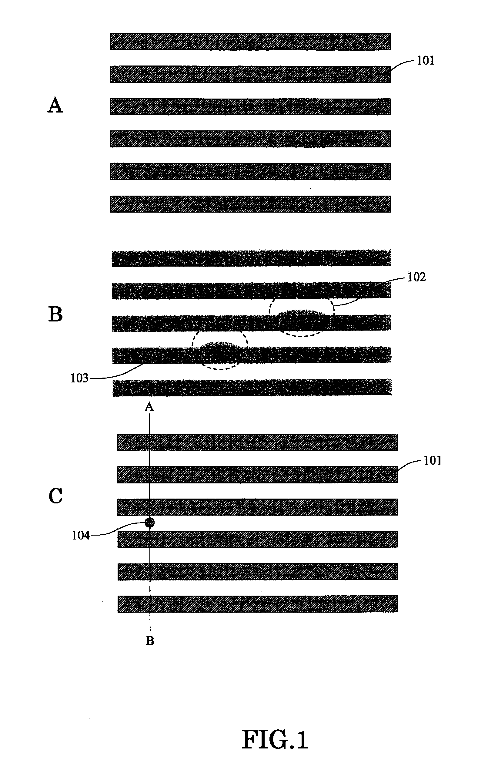
[0021]FIG. 1A represents an image of a mask pattern 101 with a plurality of lines and spaces formed on a photo mask substrate by scanning electron microscopy. fabrication process of a photo mask, it is necessary to evaluate that the photo mask fabricated by a fabrication process is good or not, namely, criteria for acceptance are satisfied or not. Ideally, the mask pattern is practically printed on a wafer by using the photo mask which is repaired and subsequently the mask pattern formed on the wafer is evaluated.

[0022]For satisfying the demand, in general, an inspection apparatus having the same wavelength and an optical system with an aligner is used. The aligner is used in printing a pattern. A pattern image is obtained by setting an illuminating condition which is the same condition with an exposure co...

second embodiment

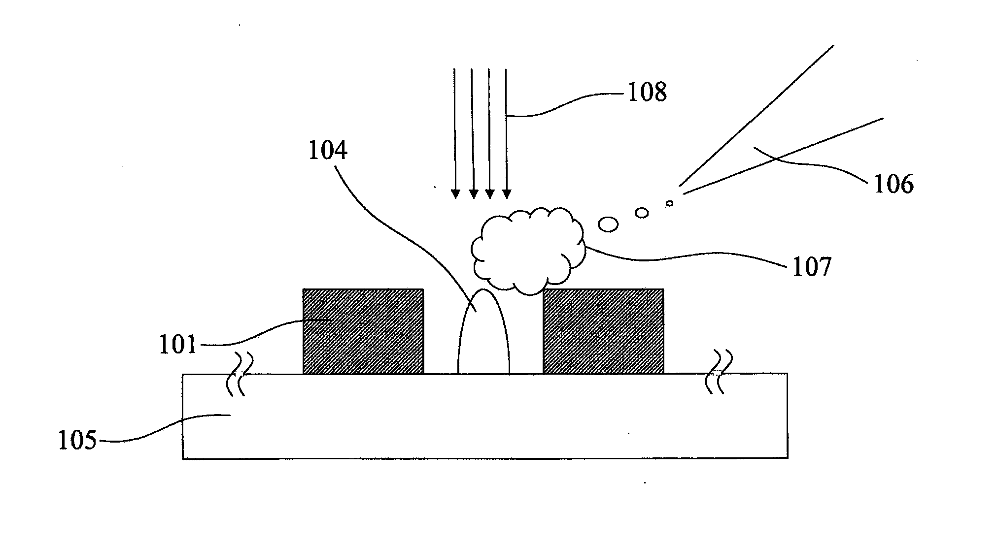
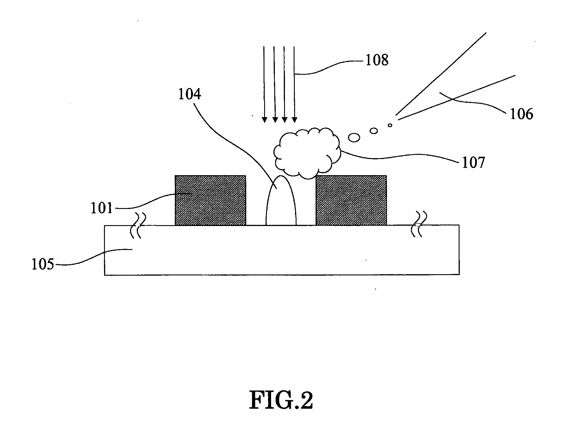
[0042]Next, a method for repairing a defect in a photo mask according to a second embodiment of the present invention will be described below in detail with reference to FIG. 7.

[0043]FIG. 7A shows an image of a mask pattern 201 with a plurality of lines and spaces formed on a photo mask substrate by scanning electron microscopy when a black defect 202 is formed over the plurality of lines and spaces. The second embodiment has a difference with the first embodiment where not only micro defects detected by an inspection apparatus but also damage defects generated on the repaired area at the previous repair process can be applied to a repairing process.

[0044]As shown in FIG. 7A, when the black defect 202 is formed over the mask pattern 201 with plurality of the lines and spaces, a portion of the black defect 202 formed on the spaces between the lines is repaired by the repair apparatus. Practically, FIB, laser, AFM, EB or the like is applied to the repairing process to remove the porti...

third embodiment

[0054]Next, a system for repairing a defect in a photo mask according to a third embodiment of the present invention will be described below in detail with reference to FIG. 8.

[0055]FIG. 8 is a block diagram showing a photo mask defect repair system in the third embodiment. A photo mask defect repair system 301 in this embodiment is constituted with an inspection apparatus portion 302, a repair apparatus portion 303, a feed portion 304, a memory portion 305, a calculation portion 306 and control portion 307.

[0056]The inspection apparatus portion 302 includes an image extraction portion 308 and a memory portion 309. The image extraction portion 308 extracting entirely same exposure condition when a device is fabricated. Therefore, a pattern image formed on a wafer is obtained when the mask pattern is printed on the wafer and information of the pattern image is stored in a memory portion 309.

[0057]The repair apparatus portion 303 is constituted with an image extraction portion 310, a ...


PUM


Abstract

There is provided a method for repairing a photo mask in this invention, including, obtaining a first image being a photo mask image including a defect area of the photo mask by a repair apparatus, obtaining a second image being a wafer printing image of the photo mask including the defect area by an inspection apparatus, superimposing the first image and the second image to identify a position of the defect area in the first image, and repairing the defect area by the repair apparatus.

Description

CROSS REFERENCE TO RELATED APPLICATION[0001]This application is based upon and claims the benefit of priority from the prior Japanese Patent Application No. JP2008-255639, filed Sep. 30, 2008; the entire contents of which are incorporated herein by reference.FIELD OF THE INVENTION[0002]The present invention relates to a method for repairing a defect in a photo mask, a system for repairing the defect in the photo mask and a program for repairing the defect in the photo mask.DESCRIPTION OF THE BACKGROUND[0003]In a fabrication process of a photo mask used in a fabrication of an integrated semiconductor circuit, a mask pattern formed on a photo mask substrate is necessary. Checking the photo mask determines that the mask pattern is good or not, in other word, criteria for acceptance are satisfied or not. As the checking method for the photo mask, observing by using an inspection apparatus having the same optical system as an aligner used for a wafer printing is an ideal approach.[0004]I...

Claims


Application Information

Patent Timeline
IPC IPC(8): G03F1/00G06K9/00G03F1/72G03F1/74
CPCG03F1/84
Inventor KANAMITSU, SHINGO
Owner KK TOSHIBA
Why Eureka
Try Eureka