Enhanced Power Distribution in an Integrated Circuit

a technology of integrated circuits and power distribution, applied in the field of semiconductor devices, can solve the problems of large overhead, large drawbacks of small memories, and large amount of die area occupied by memories, and achieve the effects of reducing the cost of ics, efficient power delivery, and small die area

Inactive Publication Date: 2010-04-22
AVAGO TECH WIRELESS IP SINGAPORE PTE
View PDF4 Cites 33 Cited by
  • Summary
  • Abstract
  • Description
  • Claims
  • Application Information

AI Technical Summary

Benefits of technology

[0006]Embodiments of the present invention provide techniques for efficiently delivering power to standard cells in an IC, including, but not limited to, latch standard cells within LBRAMs and other standard cells. Advantages of the invention include, for example, lower cost ICs resulting from standard cells and LBRAMs that are smaller in die area, increased read and write signal margins within LBRAMs, and improved levels of signal integrity in standard cells and within LBRAMs.

Problems solved by technology

However, an important issue with the use of such a large number of LBRAMs is the amount of die area occupied by the memories.
However, a disadvantage is that the sense amplifier circuits add significant area overhead, which can be a large drawback for small memories.
Furthermore, SRAMs are more susceptible to IC process defects than standard logic circuitry and may require special built-in-self-test (BIST) logic to test for such defects.

Method used


Image

  • Enhanced Power Distribution in an Integrated Circuit
  • Enhanced Power Distribution in an Integrated Circuit
  • Enhanced Power Distribution in an Integrated Circuit

Examples


Embodiment Construction

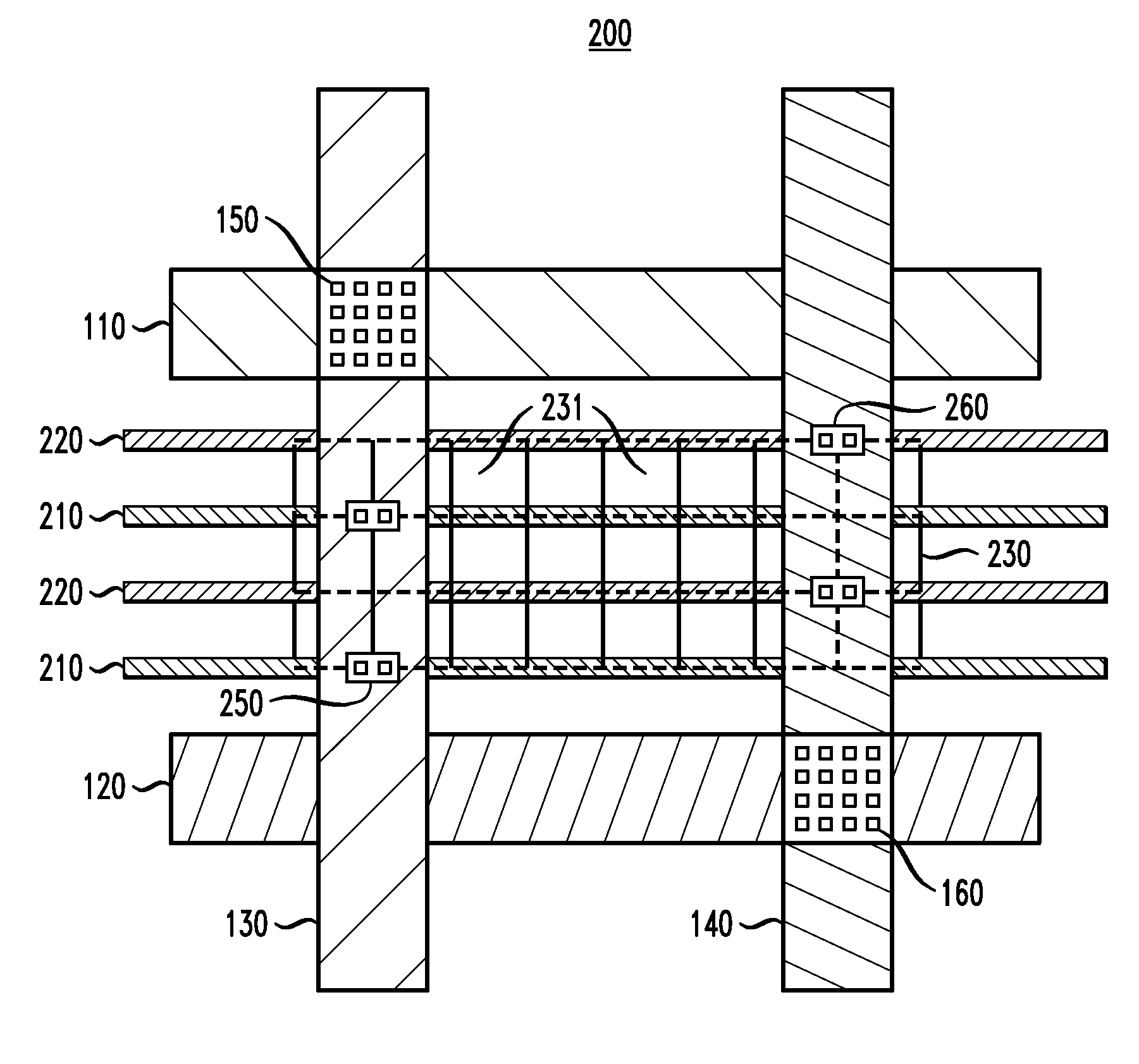
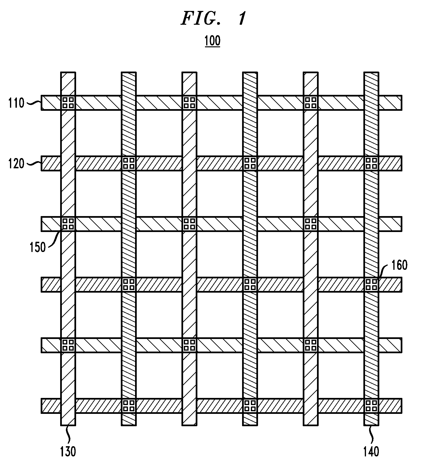
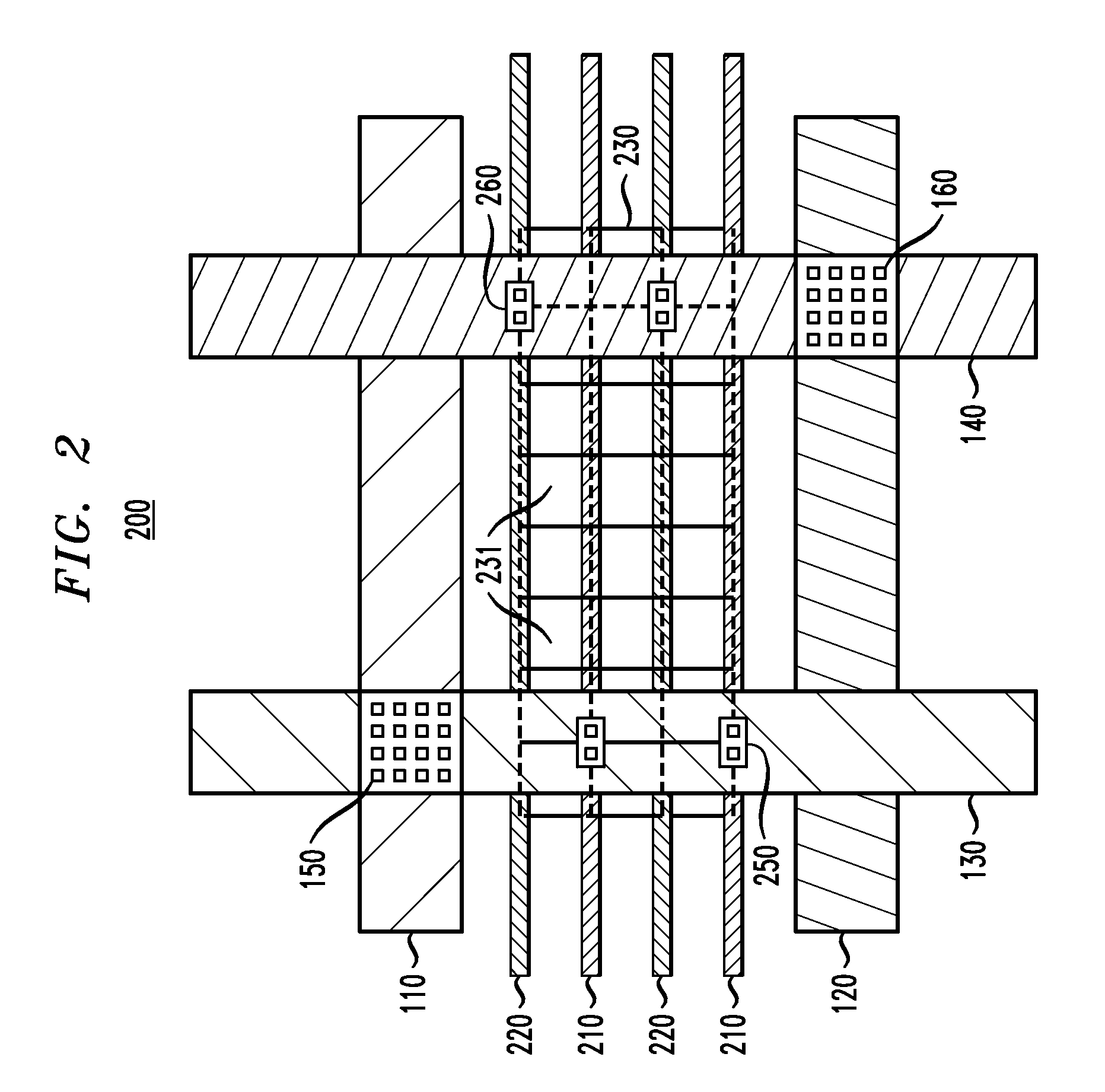
[0023]The present invention will be described herein in the context of exemplary IC power distribution layouts and methods. It is to be understood, however, that the techniques of the present invention are not limited to the IC layouts and methods shown and described herein. Rather, embodiments of the invention are directed broadly to techniques for distributing power to standard cells in an IC in a manner which provides efficient use of space so as to reduce the required die area as compared to conventional IC designs. While embodiments of the invention will be described herein in the context of LBRAM circuits comprising latch standard cells, teachings of the invention are not limited to LBRAM circuits comprising latch standard cells. Alternative embodiments of the invention may be directed to other types of standard cells in place of or in addition to LBRAM and latch standard cells, such as, for example, digital circuitry (e.g., logic circuits, flip-flops, shift registers, etc.), ...


PUM


Abstract

An integrated circuit structure for distributing power to one or more standard cells in an integrated circuit includes a first plurality of standard cells and a power mesh power connection structure coupled to the cells. Each of the standard cells includes first and second power rails adapted for connection to a voltage supply and a voltage return, respectively, of the standard cells. Each standard cell in a subset of the standard cells is arranged in direct abutment with at least two other standard cells, and at least first and second end cells are arranged in direct abutment with at least one other standard cell of the first plurality of standard cells. The power mesh power connection structure includes a plurality of conductive elements formed in a plurality of different conductive layers in the integrated circuit. The power mesh power connection structure is operative to connect the first and second power rails of the first plurality of standard cells to the voltage supply and voltage return, respectively, and is configured so as to reduce a first voltage differential between respective first power rails of the standard cells and to reduce a second voltage differential between respective second power rails of the standard cells.

Description

FIELD OF THE INVENTION[0001]The present invention relates generally to semiconductor devices, and more particularly to power distribution within an integrated circuit (IC) including memory.BACKGROUND OF THE INVENTION[0002]Recently, there is a trend for increasing memory usage in application specific integrated circuits (ASICs). The Semiconductor Industry Association (SIA) estimates that, by the year 2014, a typical ASIC will comprise about 94 percent memory (by die area). The trend is also for decreasing the size of memories, which are often implemented as latch-based random access memory (LBRAM). However, an important issue with the use of such a large number of LBRAMs is the amount of die area occupied by the memories.[0003]It is common to use static random access memories (SRAMs) within ASICs. SRAMs typically comprise bit lines, word lines and an array of special memory cells, also referred to herein as bit cells, surrounded by specialized circuitry to read data from and / or write...

Claims


Application Information

Patent Timeline
Patent Type & Authority Applications(United States)
IPC IPC(8): G11C5/14H01L21/60
CPCG11C5/063G11C8/10H01L2924/14H01L2924/1433H01L2924/19043H01L2924/30105H01L2924/0002H01L2924/30107H01L2924/3011H01L2924/00
Inventor VINKE, DAVIDDILLON, MICHAEL N.OELTJEN, BRET ALANANUMALACHETTY, UDAYANTISSERIL, THOMAS MATHEWS
Owner AVAGO TECH WIRELESS IP SINGAPORE PTE
Why Eureka
Try Eureka