

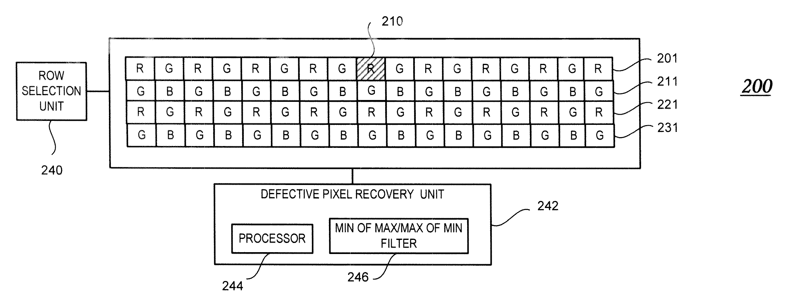
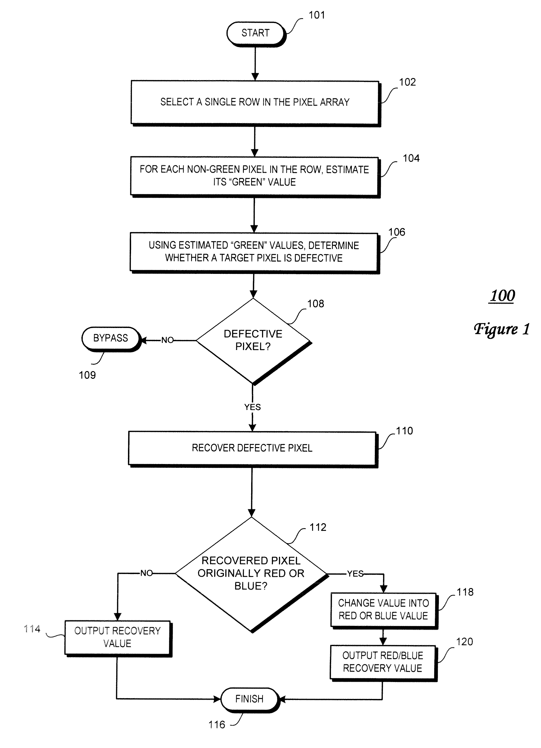
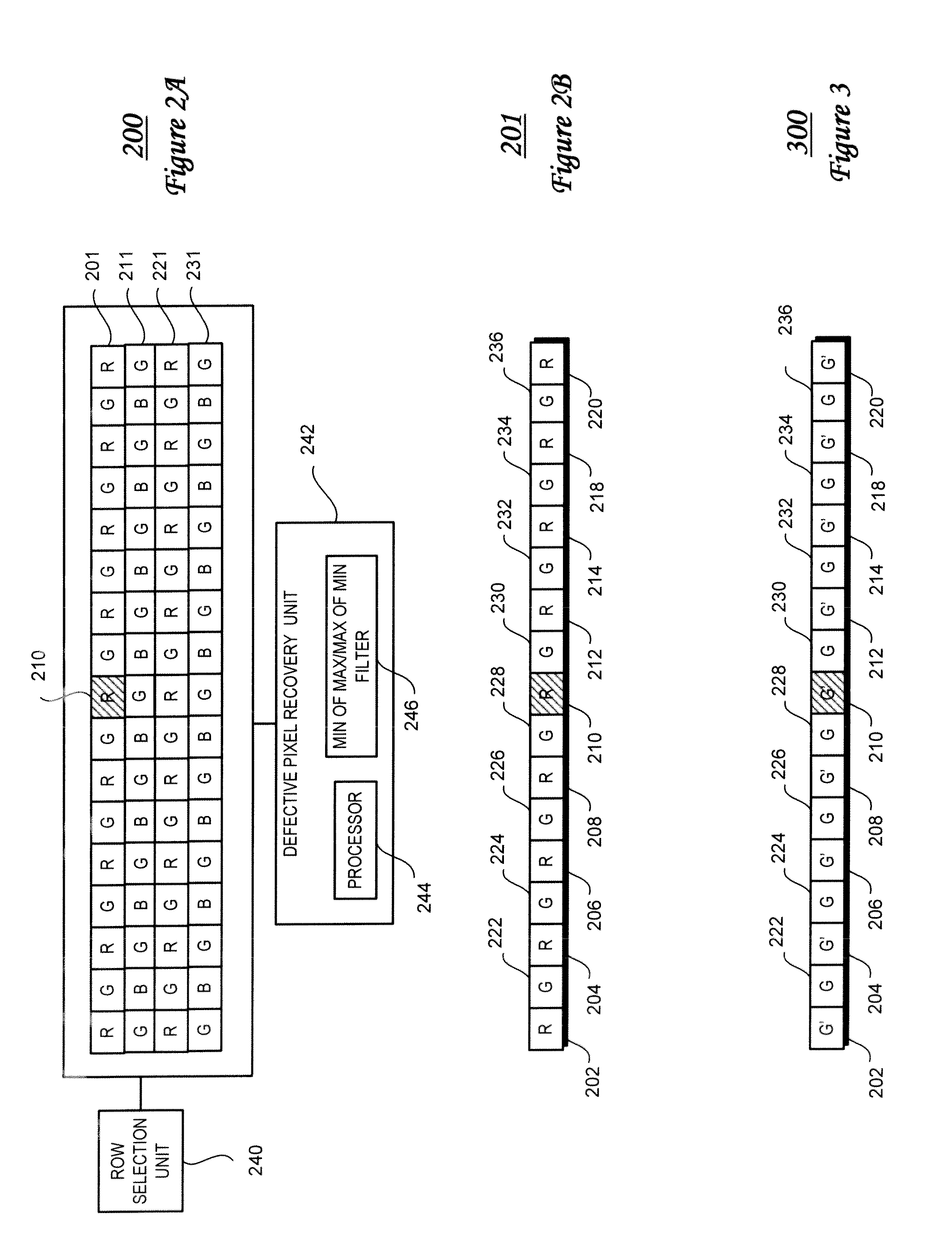
Single row based defective pixel correction
a single row and pixel correction technology, applied in the field of image sensors, can solve problems such as defective pixels in performance and yield of color image sensor devices, and limitations of conventional image sensors
- Summary
- Abstract
- Description
- Claims
- Application Information
AI Technical Summary
Benefits of technology
Problems solved by technology
Method used
Image

Examples
Embodiment Construction
[0018]In the below description, numerous specific details, such as, for example, particular processes, materials, devices, and so forth, are presented to provide a thorough understanding of embodiments of the invention. One skilled in the relevant art will recognize, however, that the embodiments of the present invention may be practiced without one or more of the specific details, or with other methods, components, etc. In other instances, structures or operations are not shown or described in detail to avoid obscuring the understanding of this description.
[0019]Reference throughout this specification to “one embodiment” or “an embodiment” means that a particular feature, structure, process, block, or characteristic described in connection with an embodiment is included in at least one embodiment of the present invention. Thus, the appearance of the phrases “in one embodiment” or “in an embodiment” in various places throughout this specification does not necessarily mean that the p...
PUM
 Abstract
Description
Claims
Application Information