Connecting unit to test semiconductor chips and apparatus to test semiconductor chips having the same

Active Publication Date: 2010-05-13
SAMSUNG ELECTRONICS CO LTD
View PDF1 Cites 2 Cited by
  • Summary
  • Abstract
  • Description
  • Claims
  • Application Information

AI Technical Summary

Benefits of technology

[0045]The controller may control connection and disconnection

Problems solved by technology

In addition, the pattern formed on the printed circuit board cannot be modified after a manufacturing process thereof.

Method used


Image

  • Connecting unit to test semiconductor chips and apparatus to test semiconductor chips having the same
  • Connecting unit to test semiconductor chips and apparatus to test semiconductor chips having the same
  • Connecting unit to test semiconductor chips and apparatus to test semiconductor chips having the same

Examples


Embodiment Construction

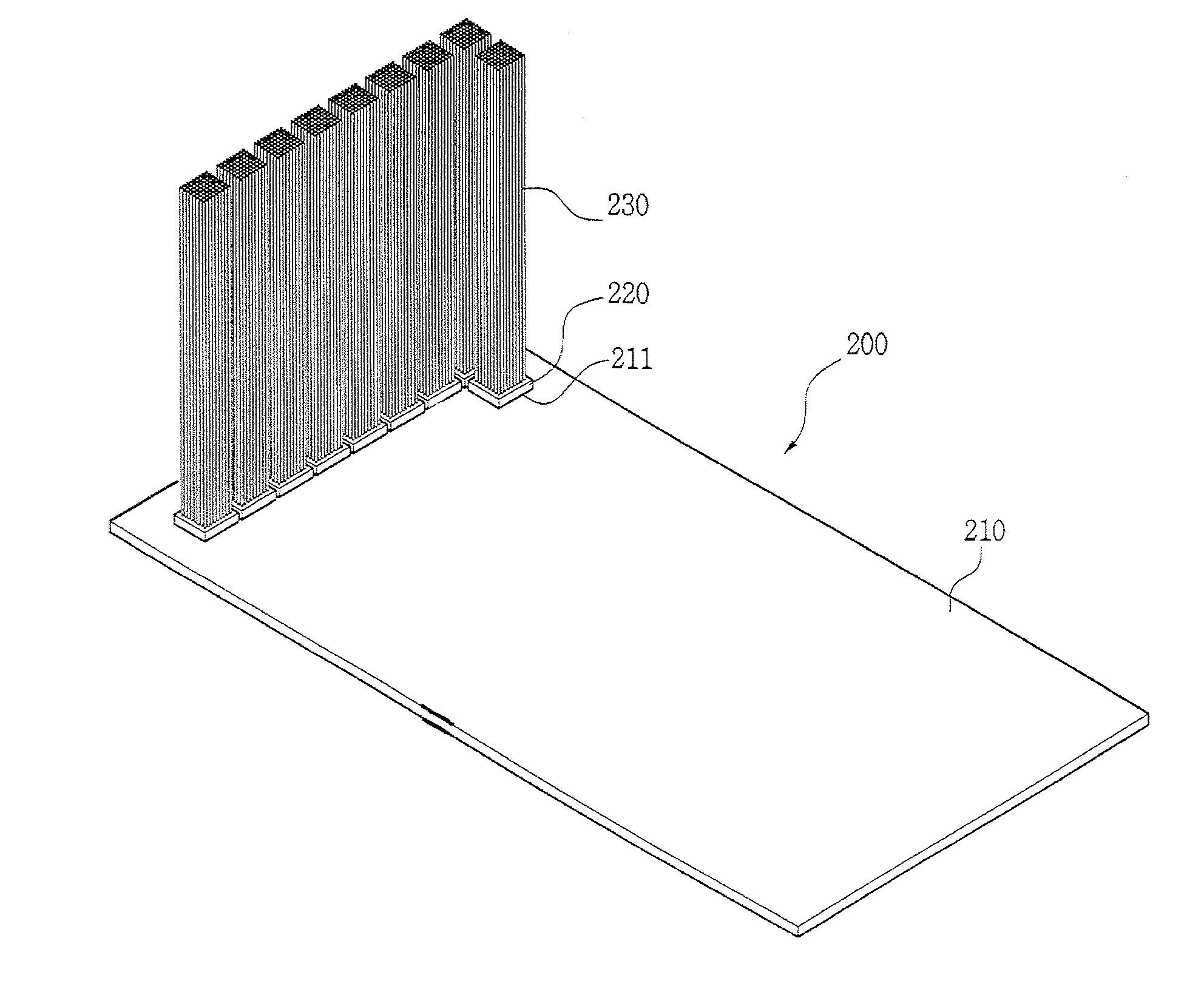
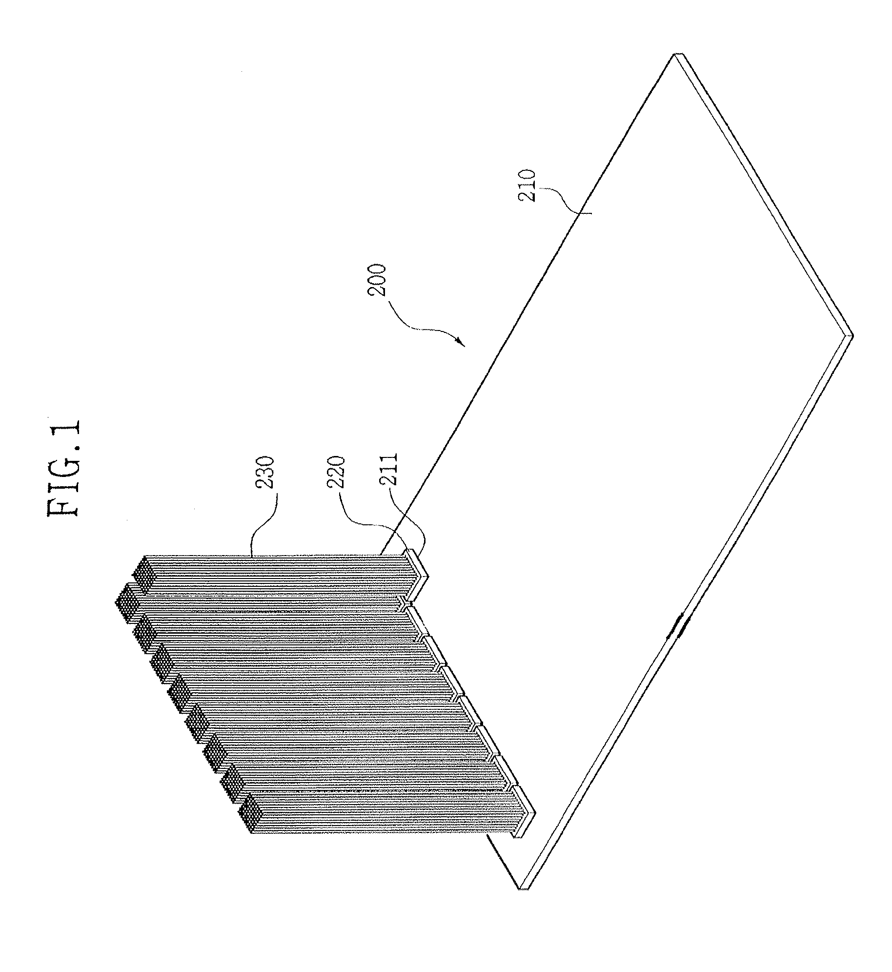
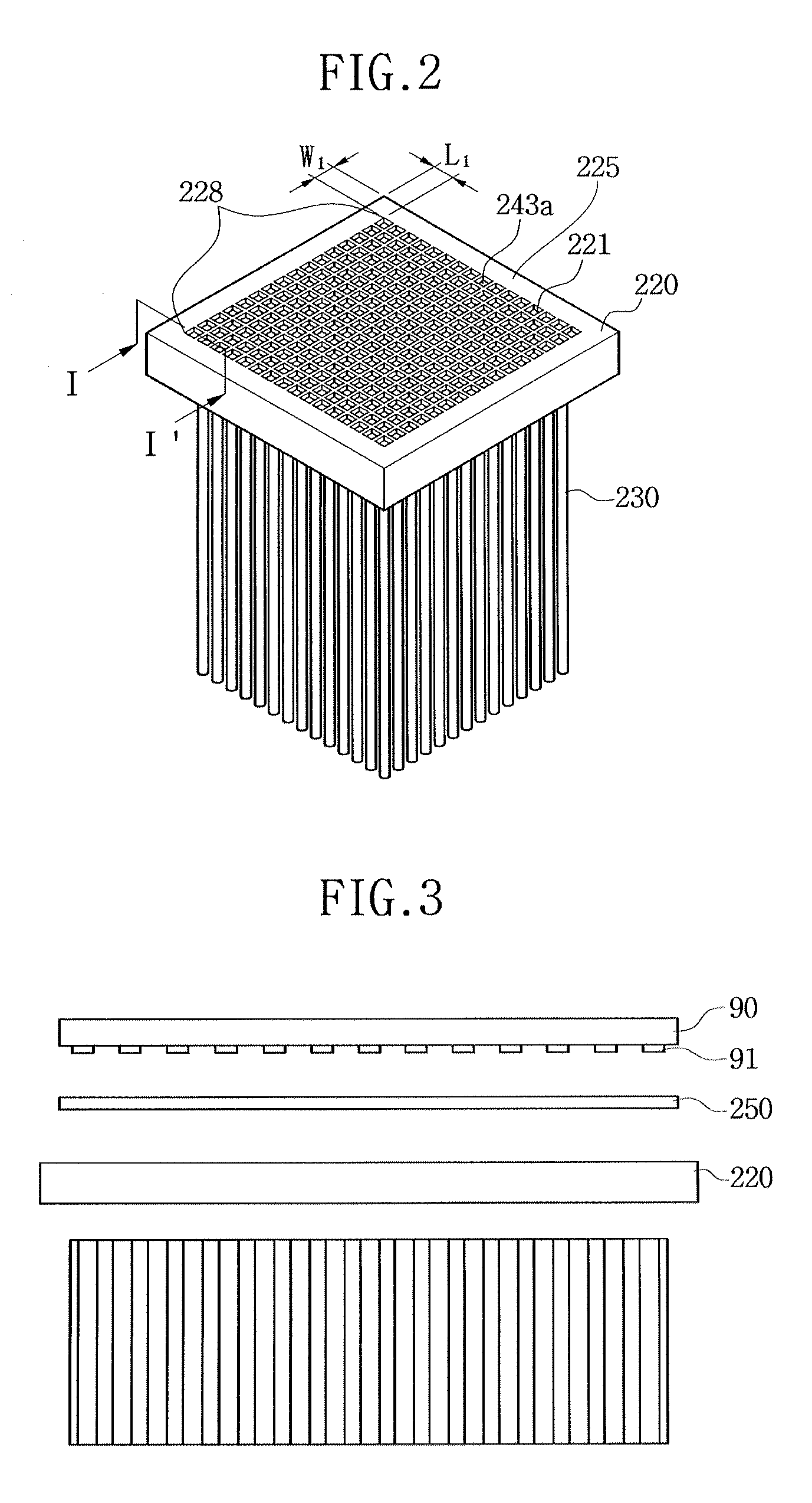
[0057]Various example embodiments will now be described more fully with reference to the accompanying drawings in which some example embodiments are illustrated, wherein like reference numerals refer to the like elements throughout. The embodiments are described below in order to explain the present general inventive concept by referring to the figures. In the drawings, the thicknesses of layers and regions may be exaggerated for clarity.

[0058]Detailed illustrative embodiments are disclosed herein. However, specific structural and functional details disclosed herein are merely representative for purposes of describing example embodiments. The present general inventive concept, however, may be embodied in many alternate forms and should not be construed as limited to only example embodiments set forth herein.

[0059]Accordingly, while example embodiments are capable of various modifications and alternative forms, embodiments thereof are illustrated by way of example in the drawings and...


PUM


Abstract

A connecting unit to test a semiconductor chip and an apparatus to test the semiconductor chip having the same include a plurality of connectors, on which a semiconductor chip having a certain pattern of electrical connection terminals, having a plurality of holes, cables configured to electrically connect the electrical connection terminals to the exterior, and coupling units configured to selectively electrically connect the cables to the electrical connection terminals through the holes. Therefore, it is possible to perform electrical tests of semiconductor chips having various patterns of electrical connection terminals and receive the semiconductor chips in a tray at a time.

Description

CROSS-REFERENCE TO RELATED APPLICATIONS[0001]This application claims priority under 35 U.S.C. §119 from Korean Patent Application No. 10-2008-0110594, filed on Nov. 7, 2008, the contents of which are hereby incorporated herein by reference in its entirety.BACKGROUND[0002]1. Field of the General Inventive Concept[0003]Example embodiments relate to an apparatus to test semiconductor chips. Other example embodiments relate to a connecting unit to test semiconductor chips and an apparatus to test semiconductor chips having the same to perform electrical tests on semiconductor chips having various patterns of electrical connection terminals and receive the semiconductor chips in a tray simultaneously.[0004]2. Description of the Related Art[0005]In general, semiconductor chips are manufactured by sequentially or selectively performing a plurality of unit processes such as deposition, diffusion, exposure, ion implantation, etc., on a wafer.[0006]Each of the semiconductor chips manufactured...

Claims


Application Information

Patent Timeline
IPC IPC(8): G01R31/02G01R31/26G01R1/06
CPCG01R31/2886G01R1/0408H01R33/76
Inventor SONG, KI-JAESEO, HUN-KYOLEE, JAE-ILHAN, JONG-WONPARK, JONG-PIL
Owner SAMSUNG ELECTRONICS CO LTD
Why Eureka
Try Eureka