Light emitting element array, drive circuit, optical print head, and image forming apparatus

a technology of drive circuit and light emitting element, which is applied in the direction of electrographic process, electrographic process apparatus, instruments, etc., can solve the problems of difficulty in reducing the size or cost of led print heads, and achieve the effects of reducing the size and cost of drive circuit, optical print heads, and reducing interferen

Active Publication Date: 2010-05-20
OKI ELECTRIC IND CO LTD
View PDF1 Cites 8 Cited by
  • Summary
  • Abstract
  • Description
  • Claims
  • Application Information

AI Technical Summary

Benefits of technology

[0011]In the present invention, instead of an LED having two terminals, the light emitting element (for example, a light emitting thyristor) has the three terminals. Gate drive circuits are consolidated in one location for driving gates of the light emitting elements with the three terminals, so that it is possible to drive the gates through the individual circuits with the level shift function per the gates of the light emitting elements with the three terminals. Accordingly, it is possible to minimize interference between the light emitting elements driven concurrently, thereby driving the light emitting elements under an ideal condition. As a result, it is possible to eliminate a power MOS transistor, thereby making it possible to reduce sizes of the drive circuit, the optical print head, and the image forming apparatus, and cost thereof.

Problems solved by technology

As a result, a chip size of the power MOS transistor increases, thereby making it difficult to reduce a size of the LED print head or cost thereof.

Method used


Image

  • Light emitting element array, drive circuit, optical print head, and image forming apparatus
  • Light emitting element array, drive circuit, optical print head, and image forming apparatus
  • Light emitting element array, drive circuit, optical print head, and image forming apparatus

Examples


first embodiment

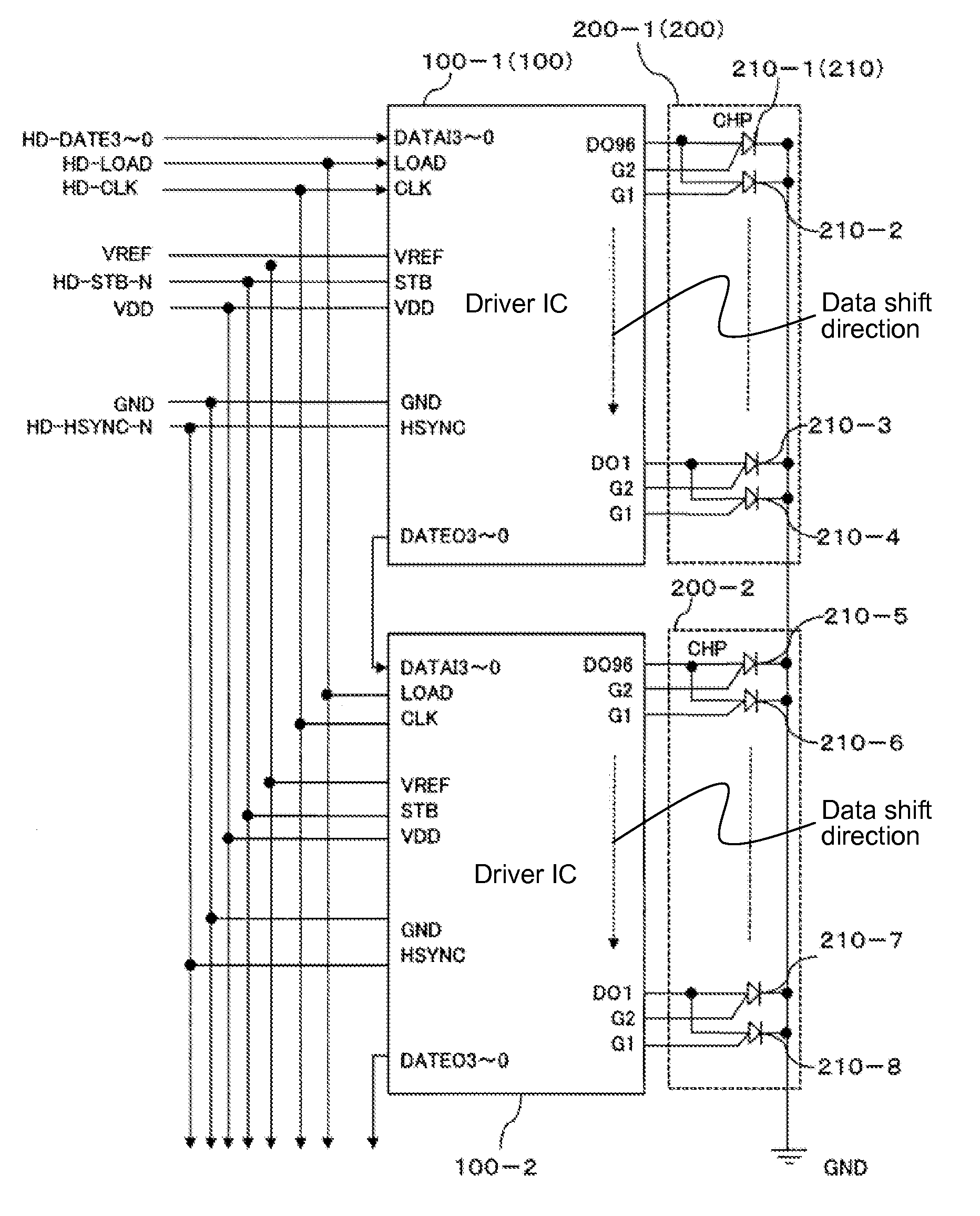
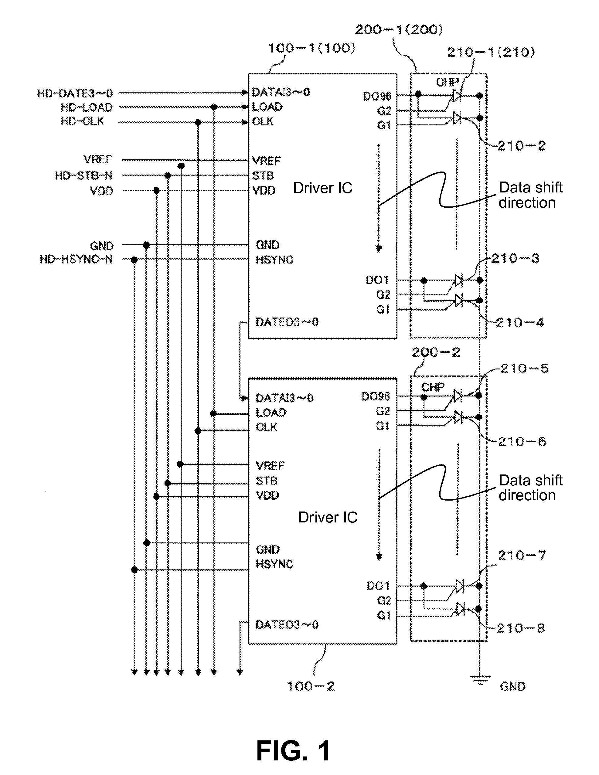
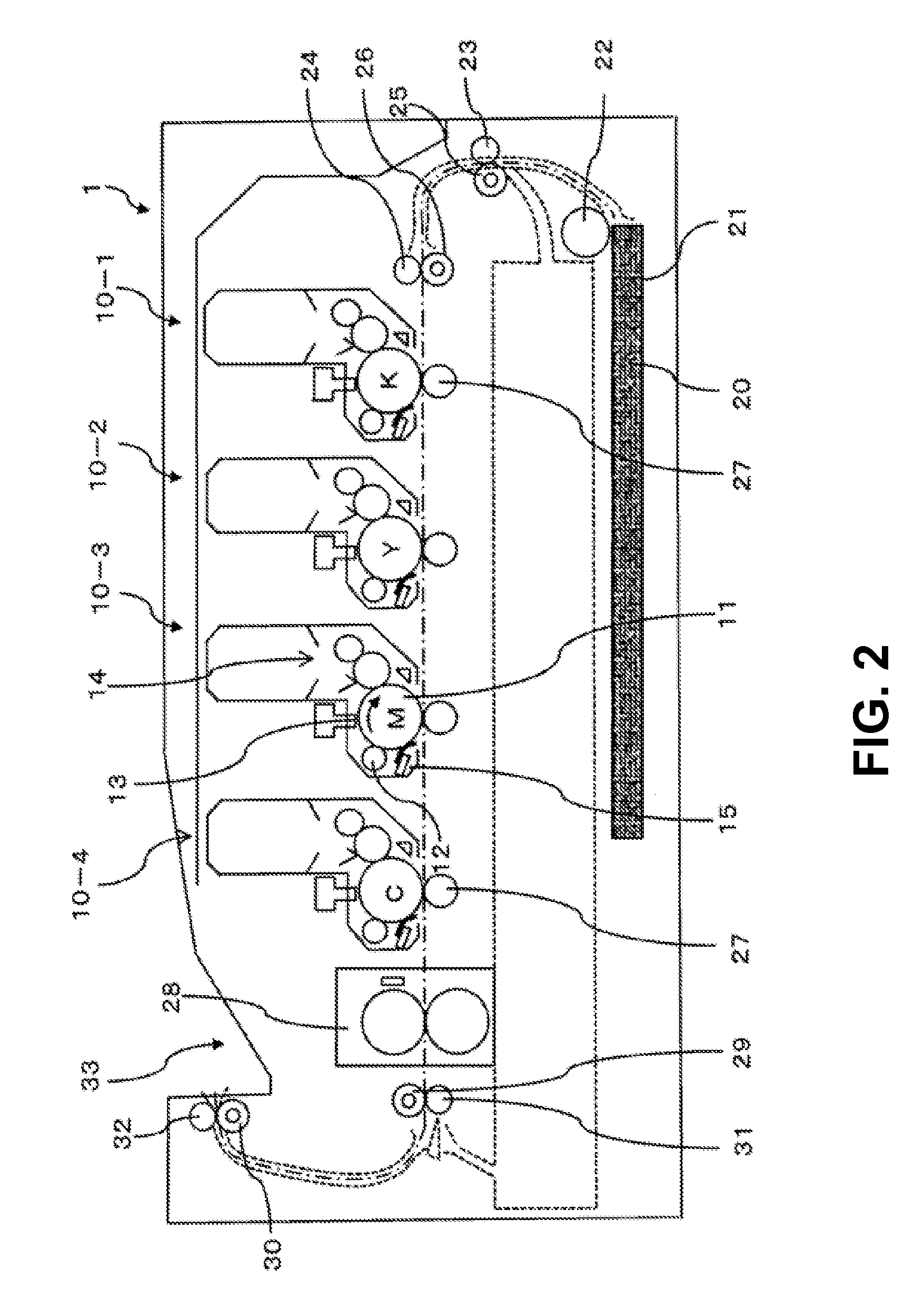
[0031]A first embodiment of the present invention will be explained. FIG. 2 is a schematic sectional view showing a configuration of an image forming apparatus 1 according to the first embodiment of the present invention.

[0032]In the embodiment, the image forming apparatus 1 is an electro-photography color printer of a tandem type provided with an optical print head having a light emitting element array using light emitting thyristors as three terminal switch elements or light emitting elements (driven elements), instead of LEDs (Light Emitting Diodes) with two terminals.

[0033]As shown in FIG. 2, the image forming apparatus 1 includes four process units 10-1 to 10-4 for sequentially forming images in colors of black (K), yellow (Y), magenta (M), and cyan (C). The process units 10-1 to 10-4 are arranged in this order along a transportation path of a recoding medium 20 (for example, a sheet) from an upstream side thereof. The process units 10-1 to 10-4 have an identical inner configur...

second embodiment

[0164]A second embodiment of the present invention will be explained next. In the second embodiment, an individual circuit 150 has a configuration different from that of the individual circuit 140 in the first embodiment shown in FIGS. 9(a) to 9(d). Configurations of the optical print head 13 having the driver ICs 100 and the image forming apparatus 1 having the optical print head 13 are similar to those in the first embodiment.

[0165]The configuration of the individual circuit 150 will be explained. FIGS. 15(a) to 15(d) are views showing the individual circuit 150 of the driver IC 100 for driving the gate according to the second embodiment of the present invention. More specifically, FIG. 15(a) is a model diagram of the individual circuit 150, FIG. 15(b) is a circuit diagram of the individual circuit 150, FIG. 15(c) is a schematic sectional view of an IC chip of the individual circuit 150, and FIG. 15(d) is an equivalent circuit diagram of the individual circuit 150.

[0166]As shown i...


PUM


Abstract

A light emitting element array includes a plurality of light emitting elements each having a first terminal, a second terminal, and a third terminal. The light emitting elements are arranged next to each other to form a group. The first terminal receives a drive signal, the second terminal is connected to ground, and the third terminal has a threshold voltage or a threshold current controllable from outside so that the light emitting elements are driven in a time division way.

Description

BACKGROUND OF THE INVENTION AND RELATED ART STATEMENT[0001]The present invention relates to a light emitting element array having a plurality of light emitting elements such as light emitting thyristors arranged therein; a drive circuit for driving the light emitting element array in a time division way; an optical print head including the light emitting element array and the drive circuit; and an image forming apparatus such as an electro-photography printer including the optical print head.[0002]In a conventional image forming apparatus (for example, an electro-photography printer using an electro-photography process), a light emitting diode (LED) print head has a plurality of LEDs arranged in a matrix pattern (refer to Patent Reference). A power MOS transistor is connected to a common connection terminal of the LEDs, so that the LEDs to be lit are switched in a time division way.[0003]Patent Reference: Japanese Patent Publication No. 2007-81081[0004]In the conventional LED print ...

Claims


Application Information

Patent Timeline
Patent Type & Authority Applications(United States)
IPC IPC(8): G03G15/04H05B37/00
CPCB41J2/45G03G15/04054G03G15/326H01L2224/48091H01L2224/49175H01L2924/00014
Inventor NAGUMO, AKIRA
Owner OKI ELECTRIC IND CO LTD
Why Eureka
Try Eureka