
Integrated circuit module and method of packaging same

a technology of integrated circuit modules and packaging methods, applied in the direction of electrical equipment, semiconductor devices, semiconductor/solid-state device details, etc., can solve the problems of insufficient shielding of high-frequency transmission lines, problematic packaging of high-frequency ic modules,

Active Publication Date: 2010-05-27
NXP USA INC
View PDF8 Cites 11 Cited by
  • Summary
  • Abstract
  • Description
  • Claims
  • Application Information

AI Technical Summary

Problems solved by technology

The packaging of high frequency IC modules has been problematic because the individual devices in such an IC module may not be adequately protected from electrical interference and the high frequency transmission lines may not be adequately shielded.

Method used


Image

  • Integrated circuit module and method of packaging same
  • Integrated circuit module and method of packaging same
  • Integrated circuit module and method of packaging same

Examples


Embodiment Construction

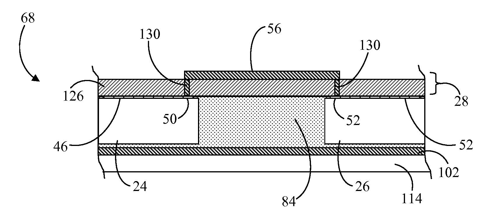
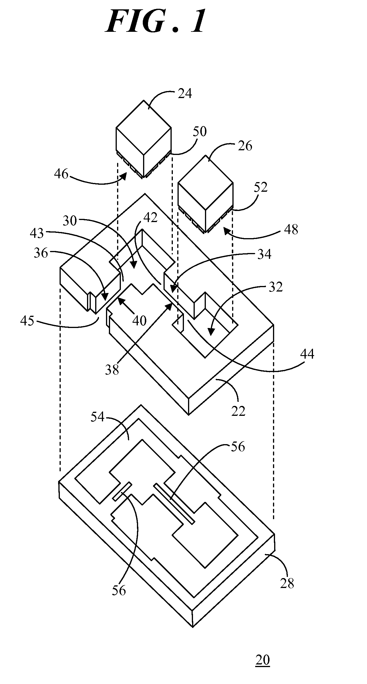
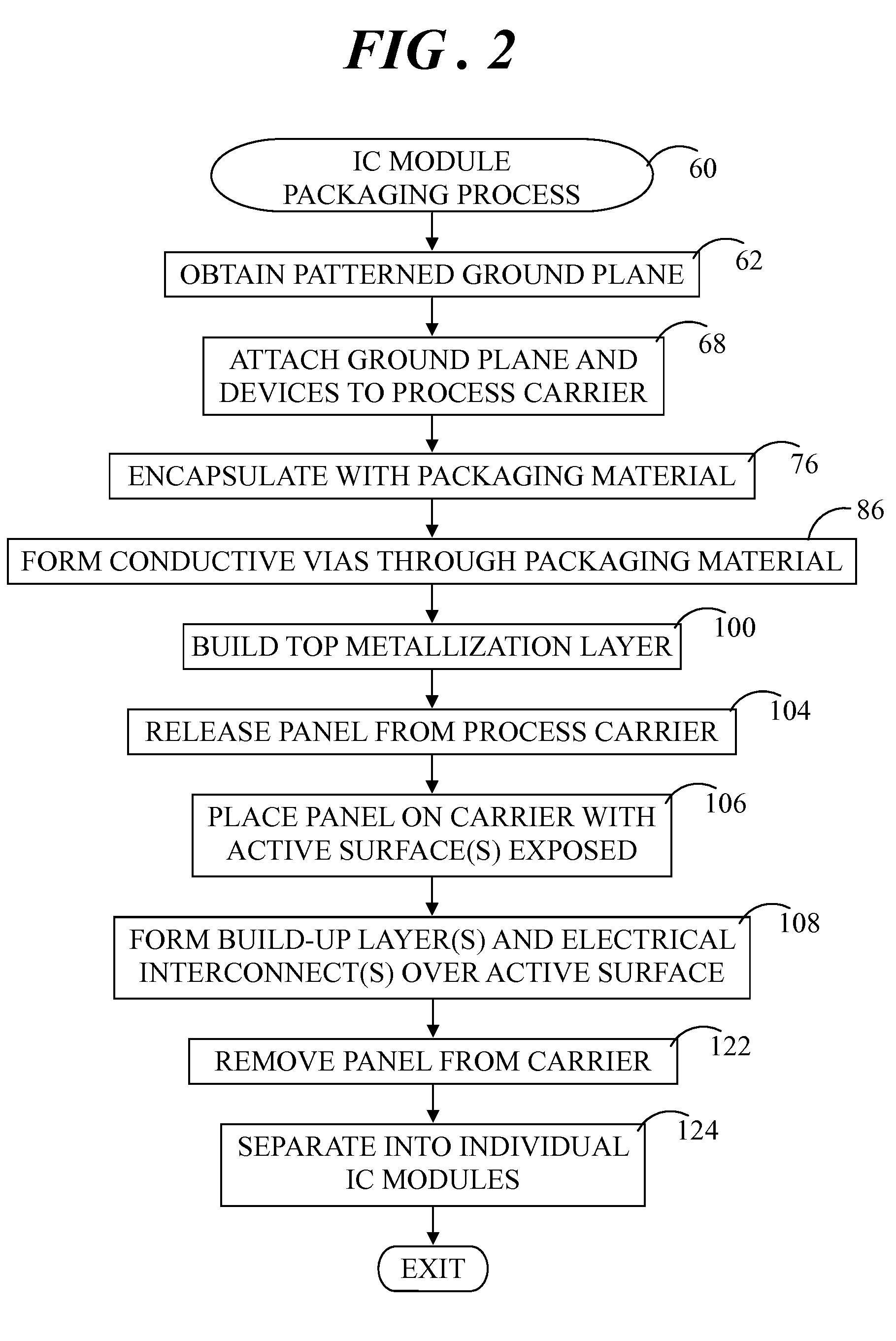
[0017]Embodiments of the invention include an integrated circuit (IC) module having one or more high frequency devices integrated therein and a method for packaging an IC module that includes one or more high frequency devices. In an embodiment, a high frequency device may be a device operating at millimeter wave, microwave, or radiofrequency wave frequencies that is suited for incorporation in various radar systems, telecommunications systems, and the like. The methodology employs a relatively low cost chips-first packaging technology that incorporates a ground plane and various structures that protect against electromagnetic interference and that provide guided signal paths for high frequency signals so as to enhance performance of the IC module relative to prior devices.

[0018]FIG. 1 shows an exploded perspective view of an integrated circuit (IC) module 20 in accordance with an embodiment of the invention. IC module 20 generally includes a ground plane 22, a device 24, a device 2...


PUM


Abstract

An integrated circuit (IC) module (20) includes a ground plane (22) having adjoining cutouts (30, 32). The cutout (32) defines a critical signal pathway (38). A device (24) is positioned in the cutout (30) and a device (26) is positioned outside of the cutout (30) adjacent to the cutout (32). An electrical interconnect (56) positioned in the critical signal pathway (38) interconnects the device (24) with the device (26). A method (60) of packaging the IC module (20) entails encapsulating the ground plane (22) and devices (24, 26) in a packaging material, and forming conductive vias (92) in the packaging material (84) that extend between the ground plane (22) and an exterior surface (94) of the packaging material (84). The conductive vias (92) surround the device (24) and cutout (32) to protect again electromagnetic interference and to provide guided signal pathways for high frequency signals on electrical interconnect (56).

Description

TECHNICAL FIELD OF THE INVENTION [0001]The present invention relates generally to integrated circuit packages. More specifically, the present invention relates to an integrated circuit module and packaging methodology for high frequency device integration.BACKGROUND OF THE INVENTION [0002]There is a continually increasing demand for radar sensors, wireless telecommunications systems, and the like that call for high frequency integrated circuit (IC) modules. Such modules include, for example, millimeter wave devices, microwave devices, radio frequency wave devices, and the like. The packaging of such modules has a significant effect on their function, their reliability, and the size of end-user devices into which the high frequency IC modules are integrated. For example, the packaging of a high frequency IC module should protect individual devices within the module from interfering with one another, protect transmission lines from interfering with one another and with surrounding dev...

Claims


Application Information

Patent Timeline
IPC IPC(8): H01L21/768H01L23/522
CPCH01L23/50H01L2924/01033H01L23/552H01L23/66H01L24/18H01L24/82H01L2224/18H01L2924/01029H01L2924/01078H01L2924/01082H01L2924/14H01L2924/19041H01L2924/3011H01L2924/3025H01L23/5389H01L21/568H01L24/19H01L2224/04105H01L2224/24137H01L2224/24195H01L2924/181H01L2924/19105H01L2924/00
Inventor TANG, JINBANG
Owner NXP USA INC
Learn More