Depletion-type NAND flash memory

a nand flash memory and nand flash technology, applied in the field can solve the problems of erroneous programming, peculiar problem of nand flash memory depletion-type, and erroneous reading in the case of reading

Active Publication Date: 2010-06-03
KIOXIA CORP
View PDF9 Cites 28 Cited by
  • Summary
  • Abstract
  • Description
  • Claims
  • Application Information

AI Technical Summary

Benefits of technology

[0012]According to an aspect of the present invention, there is provided a depletion-type NAND flash memory comprising: a NAND string composed of a plurality of serially connected depletion-type FETs; a control circuit which controls gate potentials of the plurality of depletion-type FETs in a read operation; a particular potential storage; and an adjacent memory cell threshold storage, wherein each of the plurality of depletion-type FETs is a transistor whose threshold changes in accordance with a charge quantity in a charge accumulation layer; the adjacent memory cell threshold storage stores a threshold of a source line side depletion-type FET adjacent to a source line side of a selected depletion-type FET; and the control circuit applies a potential to the gate electrode of the source line side depletion-type FET in the read operation, the applied potential being obtained by adding a particular potential stored in the particular potential storage to a threshold stored in the adjacent memory cell threshold storage.

Problems solved by technology

However, the depletion-type NAND flash memory has a peculiar problem.
As a result, reading erroneous occurs in the case of reading, and programming erroneous occurs in the case of verify-reading.

Method used


Image

  • Depletion-type NAND flash memory
  • Depletion-type NAND flash memory
  • Depletion-type NAND flash memory

Examples


first embodiment

(1) First Embodiment

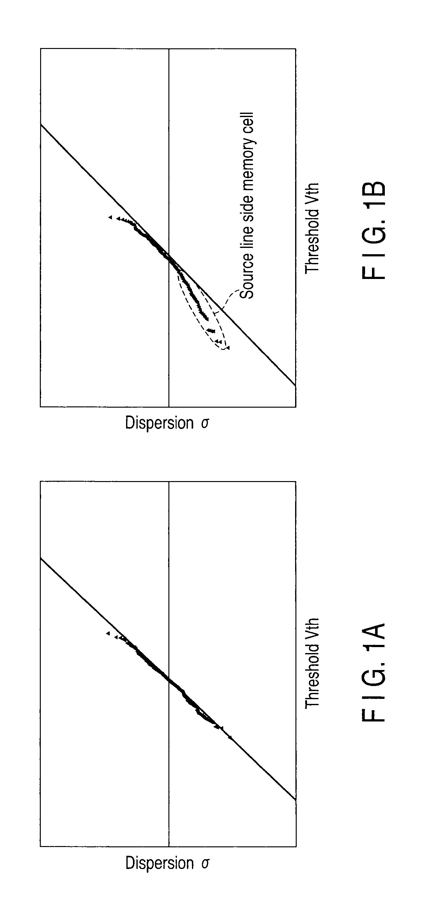
[0074]In the first embodiment, for two adjacent cells on both sides of a read target selected cell, the difference +α between a gate potential and a cell threshold is fixed, thereby preventing the variation of the threshold of the selected cell. The first embodiment corresponds to an embodiment of the first measure in the above-described principle.

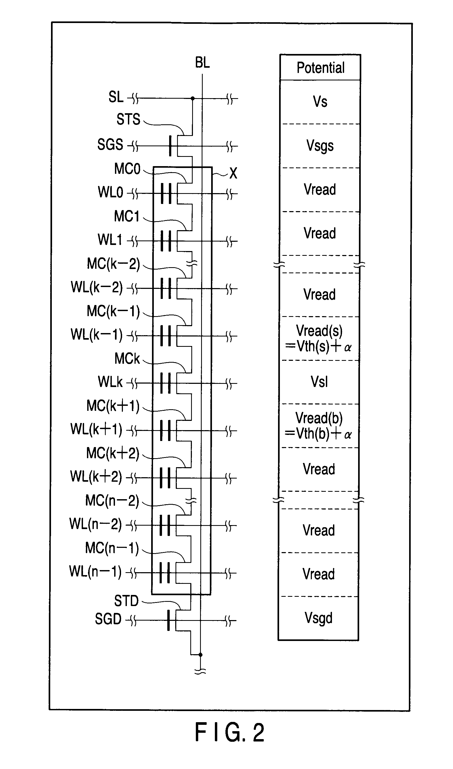
[0075]FIG. 2 shows a potential relationship in the first embodiment.

[0076]It is premised that a NAND string X is constituted of n serially connected memory cells MC0, MC1, MC2, . . . , MCk−2, MCk−1, MCk, MCk+1, MCk+2, . . . , MCn−2, MCn−1, and that each memory cell is configured by a depletion-type n-channel MOSFET.

[0077]Furthermore, a selected cell is the memory cell MCk in the read operation.

[0078]In this case, the gate potential of the selected cell MCk, that is, the potential of a word line WLk is set to a potential Vsl at which the memory cell MCk is turned on or off in accordance with a threshold Vth (sel.) of the...

second embodiment

(2) Second Embodiment

[0113]In the second embodiment, for two adjacent cells on both sides of a read target selected cell, the difference +α between a gate potential and a cell threshold is fixed, and +α is changed depending on the position of the selected cell, thereby preventing the variation of the threshold of the selected cell. The second embodiment corresponds to an embodiment of the second measure in the above-described principle.

[0114]The second embodiment is an improvement of the first embodiment and therefore includes all the characteristics of the first embodiment. Changing +α depending on the position of the selected cell is an additional characteristic of the second embodiment that is not in the first embodiment.

[0115]FIG. 6 shows a potential relationship in the second embodiment.

[0116]It is premised that a NAND string X is constituted of n serially connected memory cells MC0, MC1, MC2, . . . , MCk−2, MCk−1, MCk, MCk+1, MCk+2, . . . , MCn−2, MCn−1, and that each memory c...

third embodiment

(3) Third Embodiment

[0150]In the third embodiment, for two adjacent cells on both sides of a read target selected cell, the difference +α between a gate potential and a cell threshold is fixed, and a back bias Vbias is changed depending on the position of the selected cell, thereby preventing the variation of the threshold of the selected cell. The third embodiment corresponds to an embodiment of the third measure in the above-described principle.

[0151]The third embodiment is an improvement of the first embodiment and therefore includes all the characteristics of the first embodiment. Changing the back bias Vbias depending on the position of the selected cell is an additional characteristic of the third embodiment that is not in the first embodiment.

[0152]The back bias Vbias is first described.

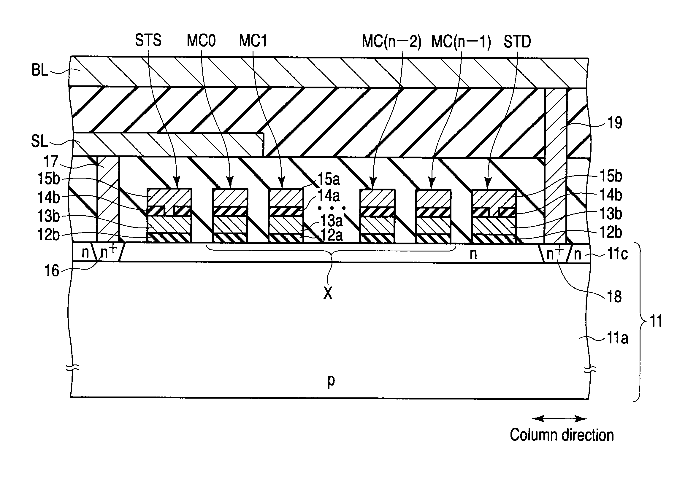
[0153]FIG. 10 shows a schematic view of a NAND string of a depletion-type NAND flash memory to which the SOI technique is applied.

[0154]An SOI substrate is composed of a p-type semiconductor r...


PUM


Abstract

A depletion-type NAND flash memory includes a NAND string composed of a plurality of serially connected FETs, a control circuit which controls gate potentials of the plurality of FETs in a read operation, a particular potential storage, and an adjacent memory cell threshold storage, wherein each of the plurality of FETs is a transistor whose threshold changes in accordance with a charge quantity in a charge accumulation layer, the adjacent memory cell threshold storage stores a threshold of a source line side FET adjacent to a source line side of a selected FET, and the control circuit applies a potential to the gate electrode of the source line side FET in the read operation, the applied potential being obtained by adding a particular potential stored in the particular potential storage to a threshold stored in the adjacent memory cell threshold storage.

Description

CROSS-REFERENCE TO RELATED APPLICATIONS[0001]This application is based upon and claims the benefit of priority from prior Japanese Patent Application No. 2008-308607, filed Dec. 3, 2008, the entire contents of which are incorporated herein by reference.BACKGROUND OF THE INVENTION[0002]1. Field of the Invention[0003]The present invention relates to a depletion-type NAND flash memory.[0004]2. Description of the Related Art[0005]A depletion-type NAND flash memory uses, as a memory cell, a depletion-type field effect transistor (FET) in which source / drain diffusion layers and a channel are of the same conductivity type (e.g., n-type). This depletion-type NAND flash memory has been attention recently owing to its suppressed short channel effect caused by shrinking (e.g., see Jpn. Pat. Appln. KOKAI Publication No. 11-163303).[0006]this depletion-type NAND flash memory has been proposed several improvements.[0007]For example, if a silicon-on-insulator (SOI) technique is applied to the depl...

Claims


Application Information

Patent Timeline
Patent Type & Authority Applications(United States)
IPC IPC(8): H01L27/088
CPCG11C16/0483H01L21/84H01L27/11521H01L27/11524H01L27/1203H01L27/11568H01L27/11578H01L27/11582H01L27/11556H10B41/35H10B41/27H10B43/30H10B41/30H10B43/20H10B43/27
Inventor MIZUKAMI, MAKOTONISHIHARA, KIYOHITO
Owner KIOXIA CORP
Why Eureka
Try Eureka