Semiconductor device

a technology of semiconductor devices and semiconductors, applied in semiconductor devices, semiconductor/solid-state device details, electrical apparatus, etc., can solve the problems of material movement and supply balance loss, disconnection failure, and b>30/b> being not disconnected, so as to mitigate the resistance distribution of electric fuse changes and stably disconn

Inactive Publication Date: 2010-06-03
RENESAS ELECTRONICS CORP
View PDF4 Cites 4 Cited by
  • Summary
  • Abstract
  • Description
  • Claims
  • Application Information

AI Technical Summary

Benefits of technology

[0023]With this structure, even when a film thickness of the first interconnect, which is designed such that the flowing-out portion is formed during the disconnection of the electric fuse, varies due to manufacturing fluctuations, a film thickness of the third interconnect also varies correspondingly to the film thickness of the first interconnect, because the third interconnect and the first interconnect are formed in the same layer. In this structure, the first interconnect and the third interconnect are arranged on the one end side and the another end side of the electric fuse, respectively. Therefore, even in a case where fluctuations in film thickness change a resistance of the first interconnect, a resistance of the third interconnect is also changed. Accordingly, change in resistance distribution of the electric fuse is mitigated. As a result, even when the fluctuations in film thickness occur, a temperature may become the highest near a connection point of the first interconnect with the first via portion as originally designed. In this way, the flowing-out portion may be formed at a constant position, and the electric fuse may be stably disconnected.

Problems solved by technology

As a result, a movement and supply balance among the materials is lost.
As a result, a disconnection failure that the via 30 is not disconnected occurs.

Method used


Image

  • Semiconductor device
  • Semiconductor device
  • Semiconductor device

Examples


Embodiment Construction

[0035]Hereinafter, an embodiment of the present invention is described with reference to the accompanying drawings. It should be noted that, throughout all the drawings, similar structural components are denoted by similar reference symbols and description thereof is appropriately omitted.

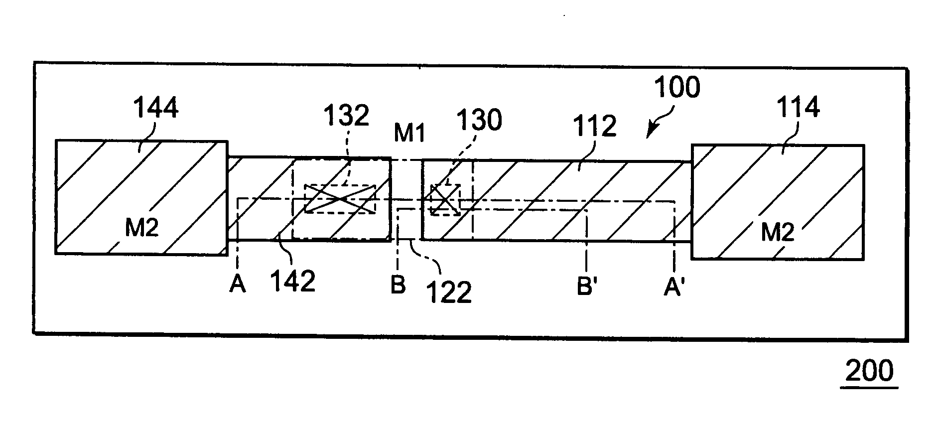
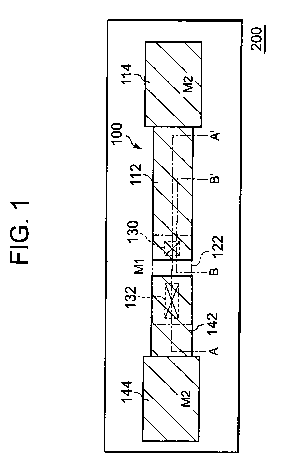
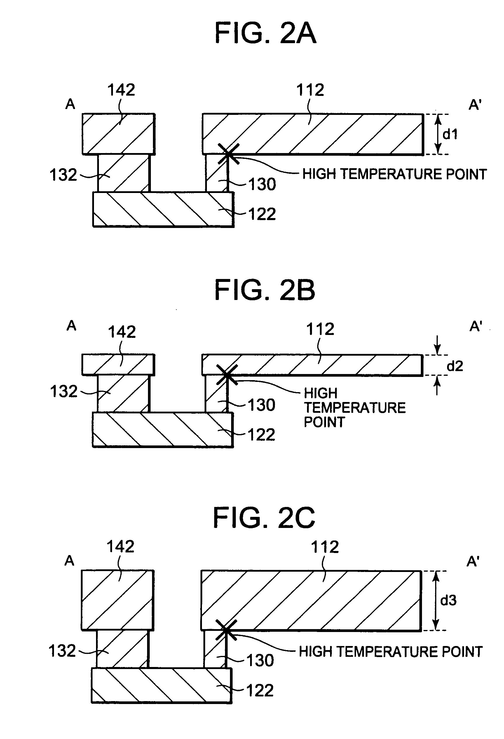
[0036]FIG. 1 is a plan view illustrating an example of a structure of a semiconductor device according to this embodiment. FIGS. 2A to 2C are cross-sectional views taken along the line A-A′ of FIG. 1. FIGS. 3A to 3C and 4A to 4C are cross-sectional views taken along the line B-B′ of FIG. 1.

[0037]A semiconductor device 200 includes a substrate (not shown) that is a semiconductor substrate such as a silicon substrate, and an electric fuse 100 formed on the substrate.

[0038]The electric fuse 100 includes: a first interconnect 112; a second interconnect 122 formed in a layer different from a layer in which the first interconnect 112 is formed; a first via 130 (first via portion) provided in contact with...


PUM


Abstract

A semiconductor device includes an electric fuse formed on a substrate. The electric fuse includes: a first interconnect formed on one end side thereof; a second interconnect formed in a layer different from a layer in which the first interconnect is formed; a first via provided in contact with the first interconnect and the second interconnect to connect those interconnects; a third interconnect formed on another end side thereof, the third interconnect being formed in the same layer in which the first interconnect is formed, as being separated from the first interconnect; and a second via provided in contact with the third interconnect and the second interconnect to connect those interconnects, the second via being lower in resistance than the first via. The electric fuse is disconnected by a flowing-out portion to be formed of a conductive material forming the electric fuse which flows outwardly during disconnection.

Description

BACKGROUND OF THE INVENTION[0001]1. Field of the Invention[0002]The present invention relates to a semiconductor device including an electric fuse.[0003]2. Description of the Related Art[0004]In recent years, there has been proposed a novel method of disconnecting an electric fuse, which is called a crack assist type method. In this method, the structure of the electric fuse, how to apply a voltage to the electric fuse, and the like are controlled, to thereby forcibly cause a conductive material forming the electric fuse as a part thereof to flow outwardly, that is, into an insulating film located around the conductive material, during disconnection of the electric fuse. As a result, a movement and supply balance among the materials is lost. In this manner, a large disconnection point is formed in another part. Accordingly, the possibility that the disconnected electric fuse is connected again may be greatly reduced, and the disconnection state may be satisfactorily maintained (see,...

Claims


Application Information

Patent Timeline
Patent Type & Authority Applications(United States)
IPC IPC(8): H01L23/525
CPCH01L23/5256H01L2924/0002H01L2924/00
Inventor KUBOTA, YOSHITAKATAKAOKA, HIROMICHITSUDA, HIROSHI
Owner RENESAS ELECTRONICS CORP
Why Eureka
Try Eureka