Active matrix substrate, liquid crystal panel, liquid crystal display unit, liquid crystal display device, television receiver, active matrix substrate manufacturing method, and liquid crystal panel manufacturing method

a technology of active matrix substrate and active matrix substrate, which is applied in the manufacture of electric discharge tubes/lamps, television systems, instruments, etc., can solve the problems of defective products and further load, and achieve the effects of reducing the open ratio, and reducing the cost of production

Active Publication Date: 2010-06-10
SHARP KK
View PDF20 Cites 29 Cited by
  • Summary
  • Abstract
  • Description
  • Claims
  • Application Information

AI Technical Summary

Benefits of technology

[0012]The present invention was made in view of the foregoing problems. An object of the present invention is to provide an active matrix substrate in a pixel segmentation system, capable of easily repairing a short-circuit between a data signal line and a scanning signal line.
[0050]As described above, with the present active matrix substrate, it is possible to repair a defect in wiring (SG leakage) without using an auxiliary line etc. Therefore, application of the present configuration to an active matrix substrate with an auxiliary line allows repairing SG leakage without the step of connecting both ends of a data signal line with the auxiliary line, and further allows avoiding the increase in load caused by connection with the auxiliary line. Application of the present configuration to an active matrix substrate without an auxiliary line allows an active matrix substrate that has been so far regarded as defective due to SG leakage to be made an acceptable product, thereby increasing the yielding ratio. These effects are particularly evident when the present configuration is applied to a large liquid crystal panel.

Problems solved by technology

However, in the liquid crystal display device of Patent Literature 2, when SG leakage occurs, an auxiliary wire must be connected with both ends of the data signal line where the SG leakage occurs, which is troublesome.
In addition, connecting the auxiliary wire results in further load.
Further, in a case of an active matrix substrate without the auxiliary wire or the source driver configured as above, when SG leakage occurs, it cannot be repaired, which results in a defective product.

Method used


Image

  • Active matrix substrate, liquid crystal panel, liquid crystal display unit, liquid crystal display device, television receiver, active matrix substrate manufacturing method, and liquid crystal panel manufacturing method
  • Active matrix substrate, liquid crystal panel, liquid crystal display unit, liquid crystal display device, television receiver, active matrix substrate manufacturing method, and liquid crystal panel manufacturing method
  • Active matrix substrate, liquid crystal panel, liquid crystal display unit, liquid crystal display device, television receiver, active matrix substrate manufacturing method, and liquid crystal panel manufacturing method

Examples


Embodiment Construction

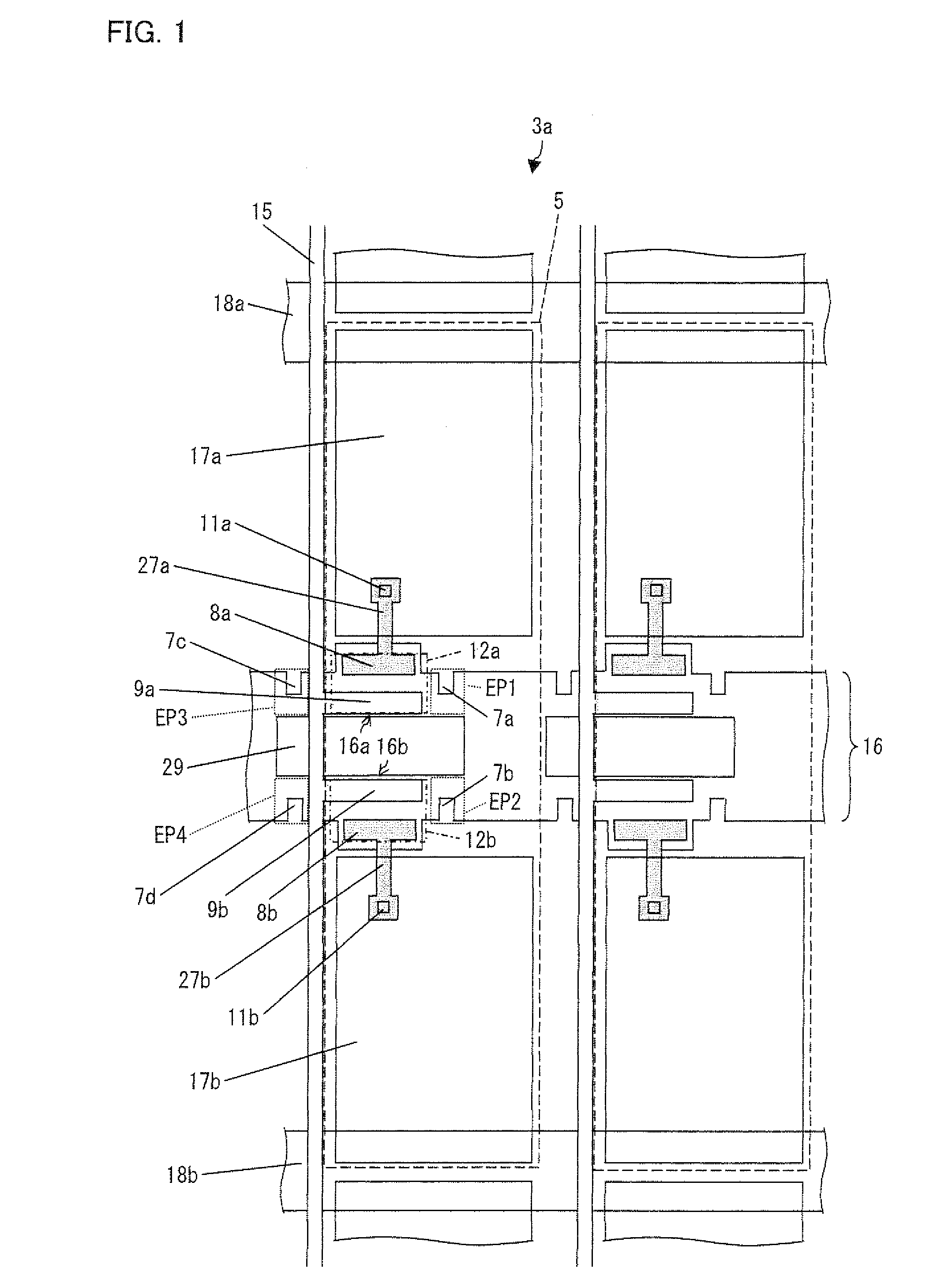
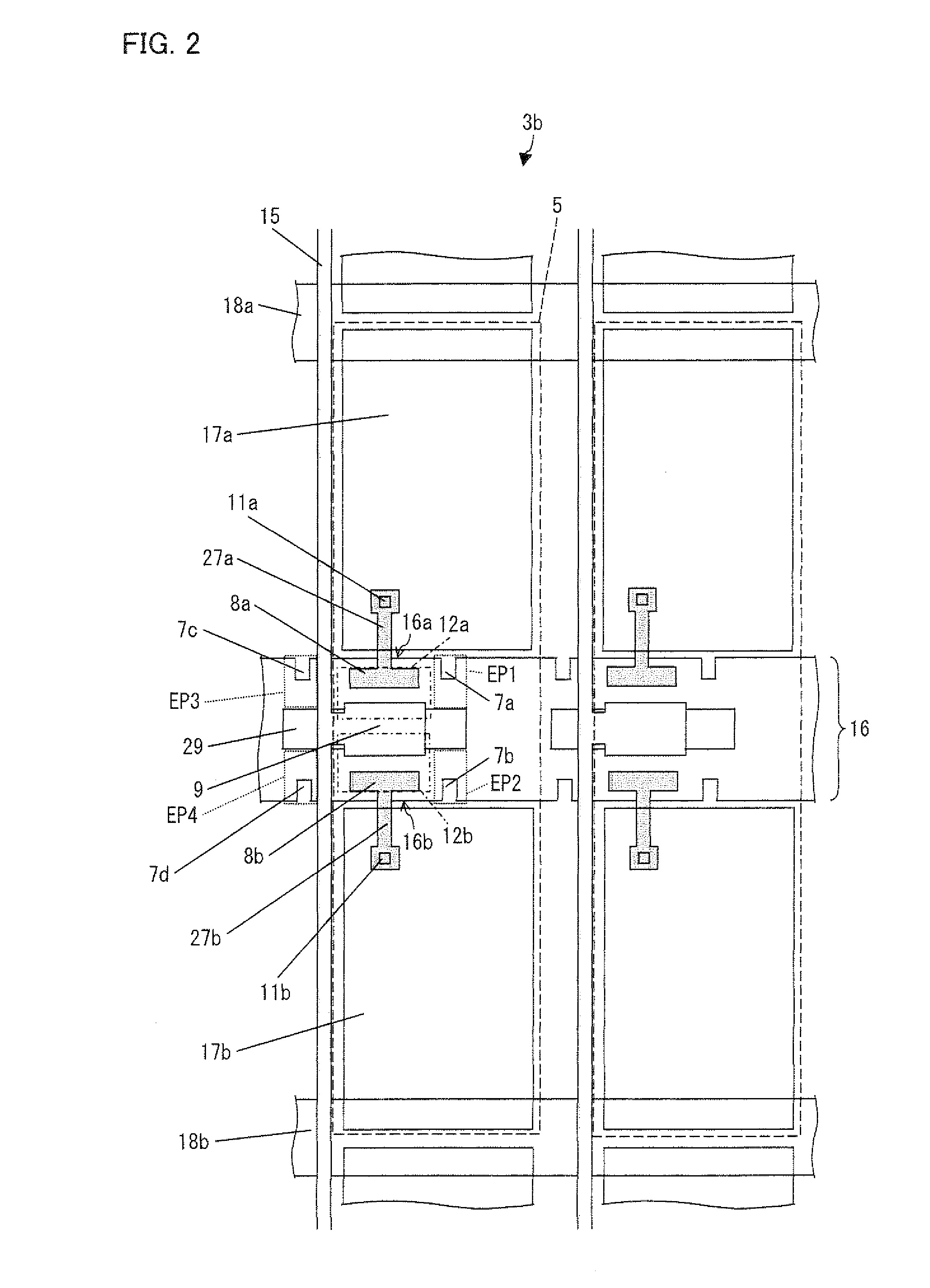
[0119]FIG. 1 is a (perspective) plan view showing a part of an active matrix substrate according to the present Embodiment of the present invention. As shown in the drawing, an active matrix substrate 3a includes data signal lines 15 and scanning signal lines 16 which intersect at right angles to each other, first and second retention capacitor wires 18a and 18b, and pixel regions 5 provided in a matrix pattern. It should be noted that a layer in which the data signal lines 15 are provided is provided above a layer in which the scanning signal lines 16 are provided. Each scanning signal line 16 extends in a row direction (horizontal direction in the drawing) so as to cross individual pixel regions 5. Each data signal line 15 extends in a column direction (vertical direction in the drawing) along edges of individual pixel regions (edges in a direction perpendicular to the scanning signal line). Each of the first retention capacitor wire 18a and the second retention capacitor wire 18b...


PUM


Abstract

A scanning signal line (16) includes an opening (29) leading from the outside of a pixel region through below a data signal line (15) into the pixel region, and first and second scanning electrode portions (16a / 16b) or two side portions of the opening confronting in a column direction through that opening. The end portion of the first scanning electrode portion (16a) in the pixel region is a first end portion (EP1), and the end portion of the second scanning electrode portion (16b) in the pixel region is a second end portion (EP2). A first transistor has a source electrode (9a) and a drain electrode (8a) individually overlapping the first electrode portion (16a) but not the first end portion (EP1) in the pixel region. A second transistor has a source electrode (9b) and a drain electrode (8b) individually overlapping the second electrode portion (16b) but not the second end portion EP2) in the pixel region. According to the aforementioned constitution, it is possible to realize a pixel split type active matrix substrate capable of easily correcting the short-circuits of the data signal line (15) and the scanning signal line (16).

Description

TECHNICAL FIELD[0001]The present invention relates to an active matrix substrate and a liquid crystal panel, capable of repairing defect in wires.BACKGROUND ART[0002]A liquid crystal display device has outstanding features such as high definition, reduced thickness, a low consumption of electricity and other features. In recent years, the market size of the liquid crystal display device has been rapidly expanding. For example, Patent Literature 1 discloses a liquid crystal display device in a pixel segmentation (multi pixel drive) system which includes a plurality of pixel electrodes in one pixel. The liquid crystal display device in the pixel segmentation system is capable of having regions with different luminance in one pixel. As a result, view angle dependency of a γ property (a difference between a γ property at a time when the liquid crystal display device is observed from front and a γ property at a time when the liquid crystal display device is observed from an oblique angle...

Claims


Application Information

Patent Timeline
Patent Type & Authority Applications(United States)
IPC IPC(8): H04N5/50G09G3/36G09G5/10H01J9/00
CPCG02F1/13624G02F2201/508G02F2001/136263G02F1/136286G02F1/136263
Inventor ENDA, KENJIITSUMI, IKUMITSUBATA, TOSHIHIDETAKEUCHI, MASANORI
Owner SHARP KK
Why Eureka
Try Eureka