Unlock instant, AI-driven research and patent intelligence for your innovation.

Semiconductor memory device and delay locked loop control method thereof

a technology of memory device and delay lock, which is applied in the direction of digital storage, pulse automatic control, instruments, etc., can solve the problems of timing mismatch between a clock outputted from a dll circuit before the start of the specific mode and a dll clock after the end of the specific mode, and achieve the effect of reducing the timing mismatch

Active Publication Date: 2010-06-10
SK HYNIX INC
View PDF6 Cites 7 Cited by
  • Summary
  • Abstract
  • Description
  • Claims
  • Application Information

AI Technical Summary

Benefits of technology

[0006]Embodiments of the present invention are directed to providing a semiconductor memory device, which reduces the timing mismatch between a DLL clock before the start of a specific mode where a DLL circuit is turned off and a DLL clock after the end of the specific mode.

Problems solved by technology

However, when a conventional power supply of a semiconductor memory device is unstable, a timing between a clock (hereinafter, referred to as a DLL clock) outputted from a DLL circuit before the start of the specific mode and a DLL clock after the end of the specific mode may be mismatched.
Due to the timing mismatch of the DLL clock, failure may occur in the semiconductor memory device.

Method used


Image

  • Semiconductor memory device and delay locked loop control method thereof
  • Semiconductor memory device and delay locked loop control method thereof
  • Semiconductor memory device and delay locked loop control method thereof

Examples


Embodiment Construction

[0017]Other objects and advantages of the present invention can be understood by the following description, and become apparent with reference to the embodiments of the present invention.

[0018]A semiconductor memory device in accordance with embodiments of the present invention turns on a DLL circuit after the start of a specific mode where the DLL circuit is turned off, and reduces the timing mismatch between a DLL clock before the start of the specific mode and a DLL clock after the end of the specific mode.

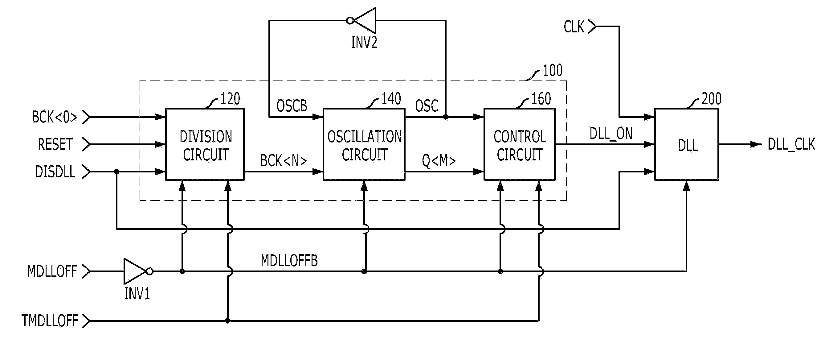
[0019]FIG. 1 is a block diagram of a semiconductor memory device in accordance with an embodiment of the present invention. Referring to FIG. 1, the semiconductor memory device in accordance with an embodiment of the present invention includes a mode control circuit 100 and a DLL circuit 200.

[0020]The mode control circuit 100 may include a division circuit 120, an oscillation circuit 140 and a control circuit 160.

[0021]The division circuit 120 divides an input clock BCK0> to ou...


PUM


Abstract

A semiconductor memory device includes a mode control circuit configured to output a DLL on signal which is periodically activated during a specific mode; and a DLL circuit configured to delay and lock a clock to generate a DLL clock, and to be periodically turned on in response to the DLL on signal during the start of the specific mode.

Description

CROSS-REFERENCE TO RELATED APPLICATIONS[0001]The present invention claims priority of Korean patent application number 10-2008-0124763, filed on Dec. 9, 2008, the disclosure of which is incorporated by reference herein in its entirety.BACKGROUND OF THE INVENTION[0002]The present invention relates to a semiconductor memory device, and more particularly, to a semiconductor memory device including a delay locked loop (DLL) circuit and a DLL control method thereof.[0003]Generally, since a high-speed semiconductor memory device processes data in synchronization with an external clock, it delays the external clock through a DLL circuit to generate an internal clock and controls the data to be outputted in accurate synchronization with the edge of the external clock.[0004]The DLL circuit does not operate in a specific mode, i.e., a power mode or a self refresh mode, and then starts to operate after the end of the specific mode.[0005]However, when a conventional power supply of a semiconduc...

Claims


Application Information

Patent Timeline
IPC IPC(8): G11C7/00G11C5/14G11C8/18H03L7/06
CPCG11C7/222G11C7/22G11C8/00
Inventor YOU, MIN-YOUNG
Owner SK HYNIX INC
Features
  • R&D
  • Intellectual Property
  • Life Sciences
  • Materials
  • Tech Scout
  • Unparalleled Data Quality
  • Higher Quality Content
  • 60% Fewer Hallucinations
Learn More