
Liquid crystal display device

Active Publication Date: 2010-06-17
PANASONIC LIQUID CRYSTAL DISPLAY CO LTD +1
View PDF5 Cites 67 Cited by
  • Summary
  • Abstract
  • Description
  • Claims
  • Application Information

AI Technical Summary

Benefits of technology

[0011]It is an object of the invention to make the gap between the TFT substrate and the counter substrate constant in the display region and the seal portion as well as to improve the reliability of the seal portion.
[0023]Further, since the sealing material is in contact with the inorganic passivation film or inter-layer insulating film formed of SiN on the TFT side, the adhesive force of the sealing material can be ensured, and the reliability of the seal portion can be improved.

Problems solved by technology

The alignment film is an organic material, so that there arises a problem of the adhesive properties between organic materials, resulting in a problem of the reliability of the seal portion.

Method used


Image

  • Liquid crystal display device
  • Liquid crystal display device
  • Liquid crystal display device

Examples


embodiment 1

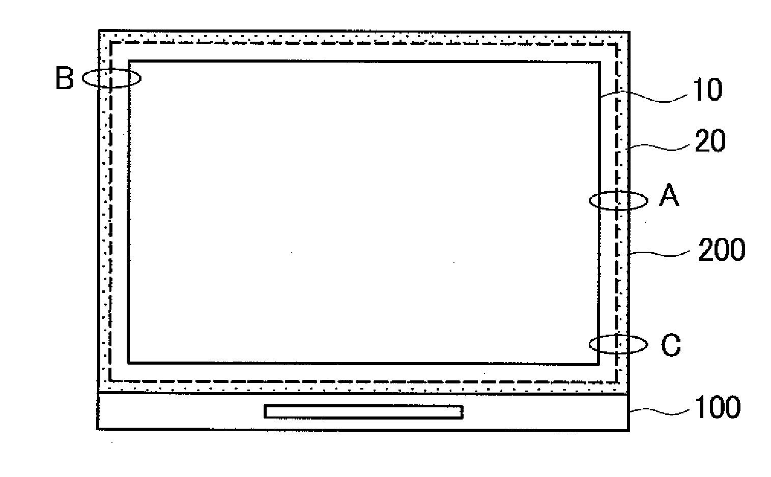
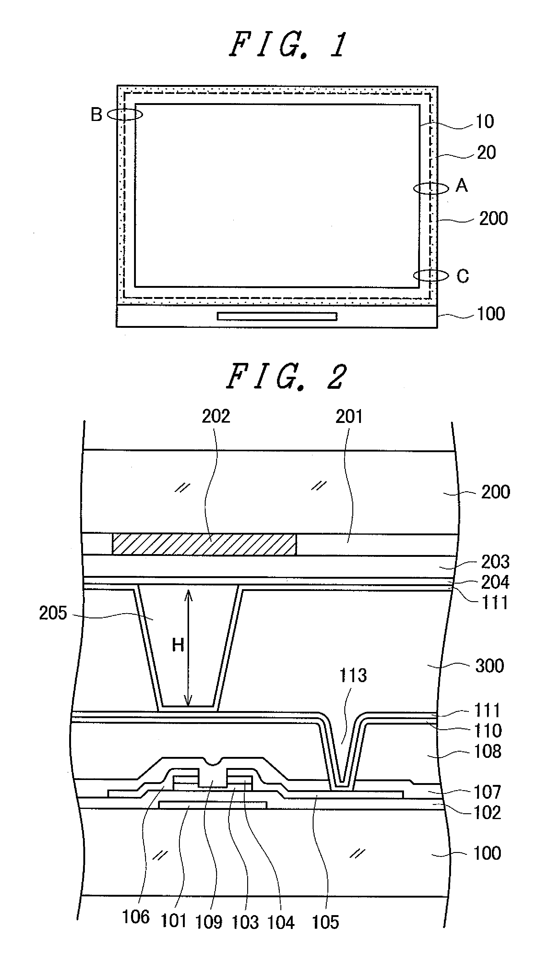
[0081]FIG. 1 is a plan view of a liquid crystal display panel according to the invention. FIG. 1 shows a small liquid crystal display panel used for a DSC (Digital Still Camera) or the like. In the liquid crystal display panel, a TFT substrate 100 having pixels formed in a matrix and a counter substrate 200 having color filters formed thereon are bonded together via a sealing material 20 at the peripheries of the substrates. The TFT substrate 100 is formed larger than the counter substrate 200. On a portion of the TFT substrate 100 where the TFT substrate 100 is larger than the counter substrate, an IC driver 30 is arranged and a terminal portion is formed.

[0082]In FIG. 1, scanning lines extend in the lateral direction on the TFT substrate 100 and routed around to the terminal portion side via scanning line lead wires on both sides of the TFT substrate. Since a frame portion outside a display region has a small width, the scanning line lead wires are formed as two-layer wiring. The ...

embodiment 2

[0132]In Embodiment 1, the TN type liquid crystal display device, which is most typical, has been described. However, the invention is not limited to the TN type liquid crystal display device but can be applied to other types. An IPS (In Plane Switching) type liquid crystal display device controls light by rotating liquid crystal molecules 301 in the horizontal direction with a lateral electric field and has excellent viewing angle characteristics.

[0133]FIG. 16 is a cross-sectional view of the display region 10 of an IPS type liquid crystal display device. Only different portions from the configuration of the typical liquid crystal display device described with reference to FIG. 2 will be described. In FIG. 16, a TFT is formed on the TFT substrate 100, and the organic passivation film 108 is formed on the inorganic passivation film 107, similarly to FIG. 2. An n+Si layer is formed on the semiconductor layer 103, but the n+Si layer is omitted in FIG. 16.

[0134]In FIG. 16, the counter ...

embodiment 3

[0147]Embodiments 1 and 2 show the examples where the organic passivation film 108 is formed on the inorganic passivation film 107. Some liquid crystal display devices use only the inorganic passivation film 107 as a protective film for a TFT without using the organic passivation film 108. The invention can also be applied to such a case.

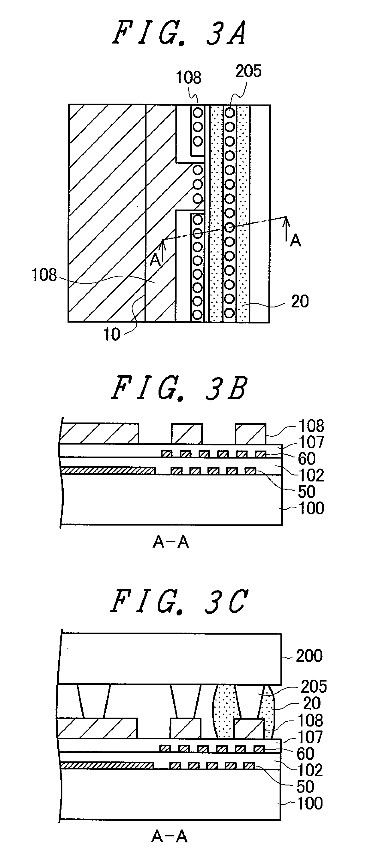
[0148]FIG. 24 is a schematic cross-sectional view of the seal portion in Embodiment 3. In FIG. 24, the column spacer 205 is formed in the seal portion, so that the column spacer 205 defines the gap between the TFT substrate 100 and the counter substrate 200 in the seal portion. Accordingly, the same gap as that in the display region 10 can be maintained.

[0149]In FIG. 24, glass fibers are not dispersed in the sealing material 20. Therefore, even when the two-layer wiring of the first scanning line lead wires 50 and the second scanning line lead wires 60 is formed in the seal portion, the inorganic passivation film 107, the gate insulating film 102, t...


PUM


Abstract

In a seal portion of a liquid crystal display device, column spacers are formed on a counter substrate side, organic passivation films are formed so as to face the column spacers on a TFT substrate side, and the gap between the TFT substrate and the counter substrate is controlled by the column spacers and the organic passivation films. A sealing material covers the column spacers and the organic passivation films and is in contact with an inorganic film formed on the TFT substrate on the TFT substrate side. Therefore, the adhesive force of the sealing material is improved to ensure the reliability of the seal portion.

Description

CROSS-REFERENCE TO RELATED APPLICATION[0001]The present application claims priority from Japanese application JP 2008-318313 filed on Dec. 15, 2008, the content of which is hereby incorporated by reference into this application.BACKGROUND OF THE INVENTION[0002]1. Field of the Invention[0003]The present invention relates to a display device and more particularly to a liquid crystal display device excellent in reliability of a seal portion.[0004]2. Description of the Related Art[0005]The uses of liquid crystal display devices have been expanded into various fields because they can be made thin. In the liquid crystal display device, a color filter substrate having color filters or the like formed at places corresponding to pixel electrodes faces a TFT substrate having the pixel electrodes, thin film transistors (TFTs), or the like formed in a matrix, and liquid crystal is interposed between the TFT substrate and the color filter substrate. The transmittance of light through liquid crys...

Claims


Application Information

Patent Timeline
IPC IPC(8): G02F1/1339G02F1/1333
CPCG02F1/133514G02F1/1339G02F1/13398G02F1/13394G02F1/1341
Inventor NAGAMI, TAKAHIRO
Owner PANASONIC LIQUID CRYSTAL DISPLAY CO LTD
Learn More