Precursor addition to silicon oxide CVD for improved low temperature gapfill

Inactive Publication Date: 2010-06-24
APPLIED MATERIALS INC
View PDF8 Cites 10 Cited by
  • Summary
  • Abstract
  • Description
  • Claims
  • Application Information

AI Technical Summary

Benefits of technology

[0008]Aspects of the disclosure pertain to methods of depositing silicon oxide layers on substrates. In embodiments, silicon oxide layers are deposited by flowing a silicon-containing precursor, an oxidizing gas, water and an additive precursor into a processing chamber such that a uniform silicon oxide growth rate is achieved across the substrate surface. The surface of silicon oxide layers grown according to embodiments may have a reduced roughness when grown with the additive precursor. In other aspects of the disclosure, silicon oxide layers are deposited on a patterned substrate with trenches on the surface by flowing a silicon-containing precursor, an oxidizing gas, water and an additive precursor into a processing chamber such that the trenches are filled with a reduced quantity and / or size of voids within the silicon oxide filler material.
[0009]In one embodiment, the present disclosure provides a method for forming a silicon oxide layer on a substrate in a processing chamber. The method includes flowing a silicon-containing precursor and flowing an oxidizing gas into the processing chamber. The method further includes flowing water and an additive precursor into the processing chamber. The silicon oxide layer is formed on the substrate from the silicon-containing precursor, the oxidizing gas, water and the additive precursor by chemical vapor deposition. The additive precursor promotes a uniform growth rate of the silicon oxide layer across the substrate and reduces roughness of the silicon oxide layer.
[0010]In another embodiment, the present disclosure provides a method for filling a trench with silicon oxide. The trench is on a substrate within a processing chamber. The method includes flowing a first silicon-containing precursor into the processing chamber. The first silicon-containing precursor comprises at least one Si—O bond. The method further includes flowing an oxidizing precursor, water and a second silicon-containing precursor into the chamber. The second silicon-containing precursor comprises at least one Si—C bond. The method further includes depositing the silicon oxide in the trench with the first and second silicon-containing precursors and the oxidizing precursor by chemical vapor deposition. The second precursor evens out a growth rate, thereby reducing a size of voids and / or a number of voids which remain in the trench following deposition.

Problems solved by technology

A challenge associated with the formation of sub-micron devices is filling a narrow trench in a void-free manner.
However, as the trench becomes narrower, even reflow processes may have difficulty filling the void.
Moreover, several types of applications call for the deposition of lightly or undoped silicon oxide, which can be difficult to reflow even at an elevated temperature.
Voids resulting from pinching-off are undesirable as they can reduce the performance and yield of good chips per wafer as well as the reliability of the devices.
Using similar precursors at lower substrate temperatures results in spatially varying film growth rates.
Film growth rate irregularities can act to trap voids within a trench thereby reducing the benefits of using a TEOS / Ozone process.

Method used


Image

  • Precursor addition to silicon oxide CVD for improved low temperature gapfill
  • Precursor addition to silicon oxide CVD for improved low temperature gapfill
  • Precursor addition to silicon oxide CVD for improved low temperature gapfill

Examples


Embodiment Construction

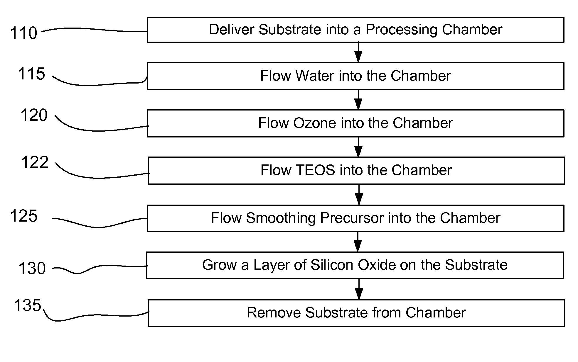
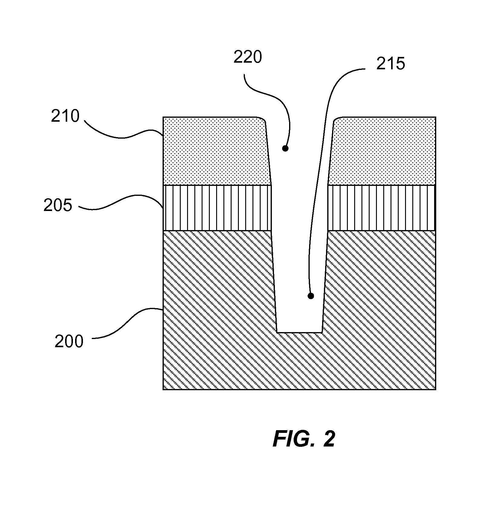
[0020]Aspects of the disclosure pertain to methods of depositing silicon oxide layers on substrates. In embodiments, silicon oxide layers are deposited by flowing a silicon-containing precursor, an oxidizing gas, water and an additive precursor into a processing chamber such that a uniform silicon oxide growth rate is achieved across the substrate surface. The surface of silicon oxide layers grown according to embodiments may have a reduced roughness when grown with the additive precursor. In other aspects of the disclosure, silicon oxide layers are deposited on a patterned substrate with trenches on the surface by flowing a silicon-containing precursor, an oxidizing gas, water and an additive precursor into a processing chamber such that the trenches are filled with a reduced quantity and / or size of voids within the silicon oxide filler material.

[0021]Embodiments of the invention are directed to methods of forming silicon oxide in trenches on a patterned surface of a substrate. An ...


PUM

PropertyMeasurementUnit
Temperatureaaaaaaaaaa

Abstract

Methods of depositing silicon oxide layers on substrates involve flowing a silicon-containing precursor, an oxidizing gas, water and an additive precursor into a processing chamber such that a uniform silicon oxide growth rate is achieved across the substrate surface. The surface of silicon oxide layers grown according to embodiments may have a reduced roughness when grown with the additive precursor. In other aspects of the disclosure, silicon oxide layers are deposited on a patterned substrate with trenches on the surface by flowing a silicon-containing precursor, an oxidizing gas, water and an additive precursor into a processing chamber such that the trenches are filled with a reduced quantity and / or size of voids within the silicon oxide filler material.

Description

CROSS-REFERENCES TO RELATED APPLICATIONS[0001]This application claims the benefit of U.S. Provisional Application No. 61 / 138,864 by Venkataraman et al, filed December 19, 2008 and titled “PRECURSOR ADDITION TO SILICON OXIDE CVD FOR IMPROVED LOW TEMPERATURE GAPFILL” which is incorporated herein in its entirety for all purposes.FIELD[0002]This application relates to manufacturing technology solutions involving equipment, processes, and materials used in the deposition, patterning, and treatment of thin-films and coatings, with representative examples including (but not limited to) applications involving: semiconductor and dielectric materials and devices, silicon-based wafers and flat panel displays (such as TFTs).BACKGROUND OF THE INVENTION[0003]The fabrication sequence of integrated circuits often includes several patterning processes. The patterning processes may be used to define a layer of conducting features which may be formed in metal, polysilicon or doped silicon. Thereafter,...

Claims


Application Information

Patent Timeline
IPC IPC(8): H01L21/31H01L21/762
CPCC23C16/401H01L21/02164H01L21/02211H01L21/76224H01L21/02222H01L21/02271H01L21/31612H01L21/02216H01L21/02274
Inventor VENKATARAMAN, SHANKARHAMANA, HIROSHIHERNANDEZ, MANUEL A.INGLE, NITIN K.GEE, PAUL EDWARD
Owner APPLIED MATERIALS INC
Why Eureka
Try Eureka