Display apparatus
a technology of display apparatus and display image, which is applied in the field of display apparatus, can solve the problems of difficult for a light receiving element provided on a tft array substrate to receive visible light emitted from a detection object, difficulty in detecting objects, and light to be transmitted through, so as to improve image quality and position detection accuracy
- Summary
- Abstract
- Description
- Claims
- Application Information
AI Technical Summary
Benefits of technology
Problems solved by technology
Method used
Image
Examples
embodiment 1
Configuration of the Liquid Crystal Display Apparatus
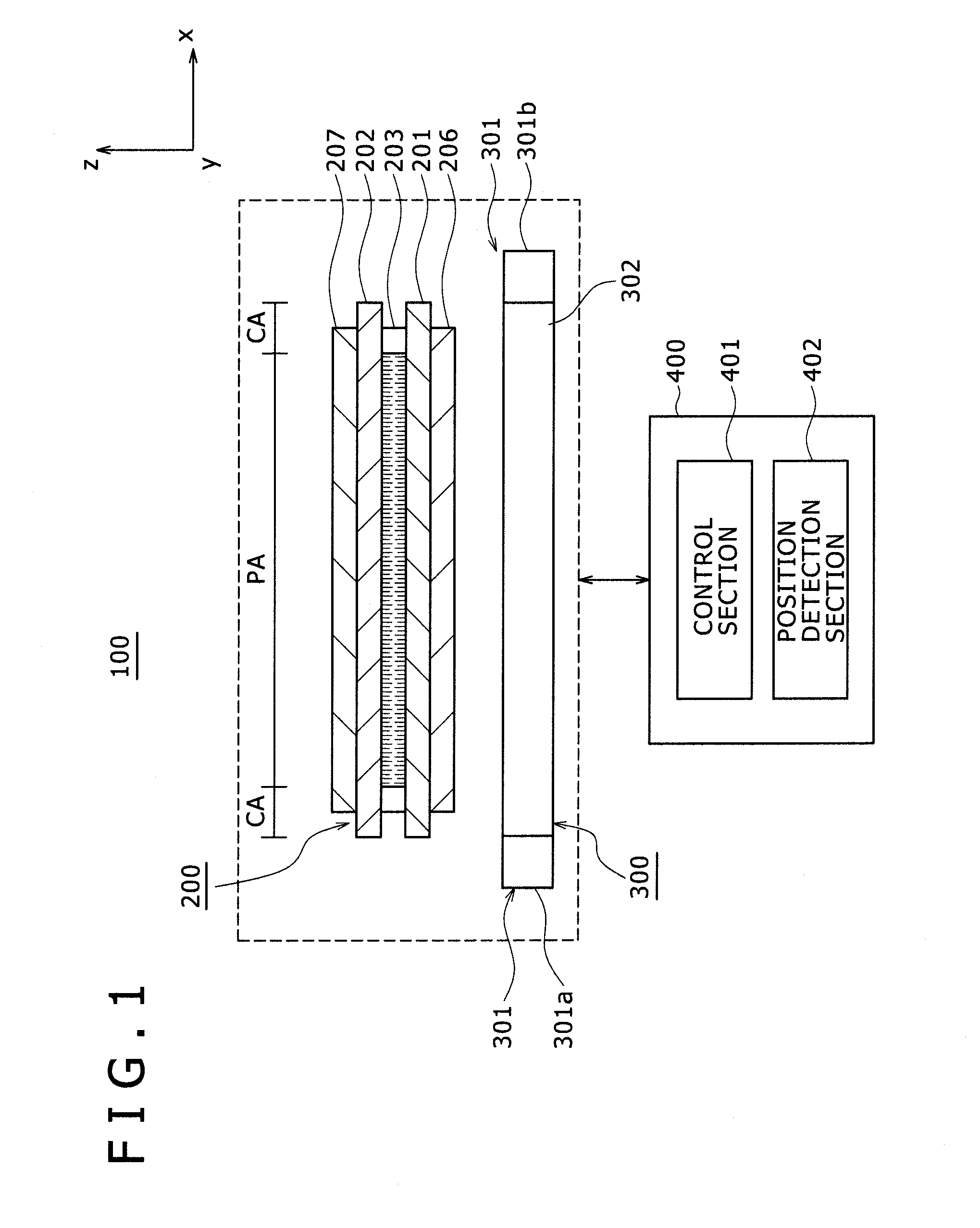
[0055]FIG. 1 is a sectional view showing a configuration of a liquid crystal display apparatus 100 in an embodiment 1 according to the present invention.
[0056]As shown in FIG. 1, the liquid crystal display apparatus 100 of the present embodiment has a liquid crystal panel 200, a backlight 300 and a data processing section 400. The components are described successively.
[0057]The liquid crystal panel 200 is of the active matrix type and has a TFT array substrate 201, an opposing substrate 202 and a liquid crystal layer 203 as shown in FIG. 1.
[0058]In this liquid crystal panel 200, the TFT array substrate 201 and the opposing substrate 202 are opposed to each other with a distance placed therebetween. The liquid crystal layer 203 is provided in such a manner as to be sandwiched between the TFT array substrate 201 and the opposing substrate 202.
[0059]Further, as shown in FIG. 1, in the liquid crystal panel 200, a first polarizing plat...
embodiment 2
[0181]In the following, an embodiment 2 according to the present invention is described.
[0182]In the present embodiment, band gaps of semiconductor layers of the position sensor elements 32a and the external light sensor elements 32b are different from each other. Except this point, the present embodiment is similar to the embodiment 1. Therefore, description of overlapping portions is omitted.
[0183]In the present embodiment, a semiconductor layer in which the position sensor elements 32a receive and photoelectrically convert reflected light of a detection object body and another semiconductor layer in which the external light sensor elements 32b receive and photoelectrically convert external light have band gaps different from each other.
[0184]Here, the semiconductor layer in which photoelectric conversion is carried out by the position sensor elements 32a is formed such that it has a band gap narrower than that of the semiconductor layer in which photoelectric conversion is carrie...
embodiment 3
[0192]In the following, an embodiment 3 according to the present invention is described.
[0193]FIG. 24 is a plan view schematically illustrating a manner wherein light receiving elements 32 are disposed in a display region PA in a liquid crystal panel 200c in the embodiment 3 according to the present invention.
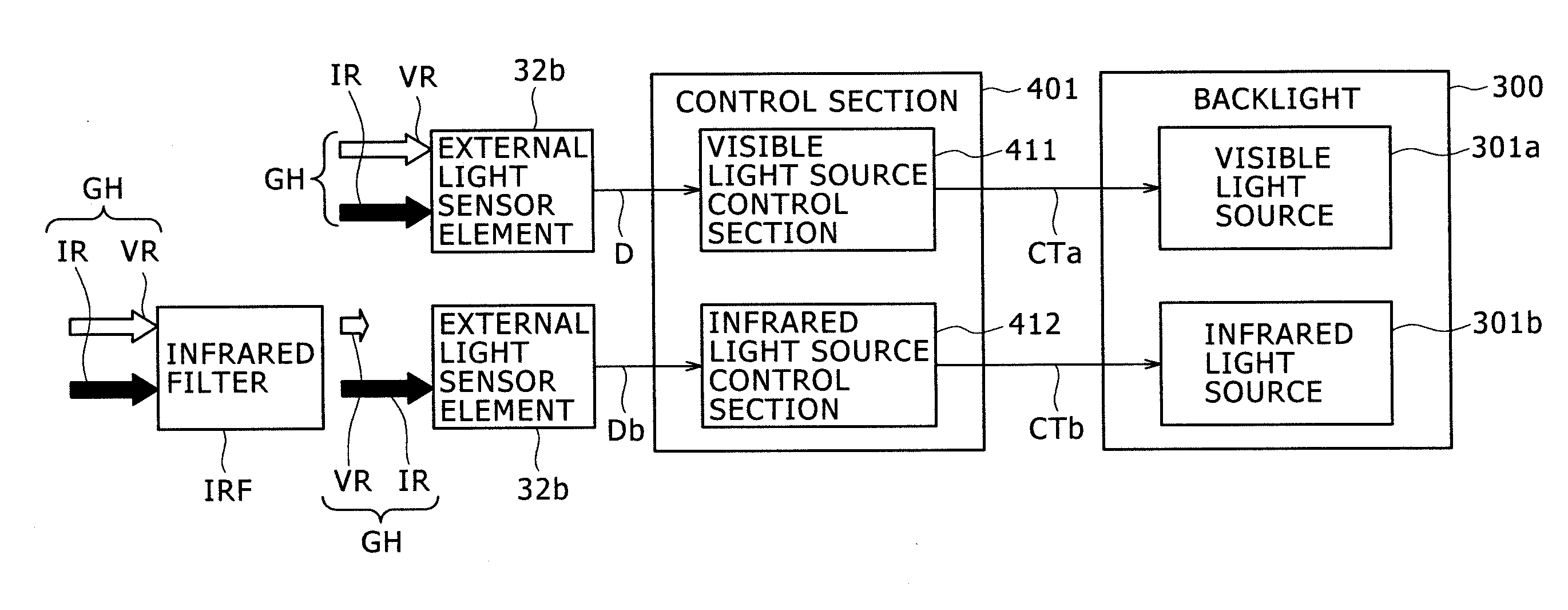
[0194]Meanwhile, FIG. 25 is a block diagram conceptually illustrating inputting / outputting of data between principal components of a control section 401 and other members in the embodiment 3 according to the present invention.
[0195]The present embodiment is different from the embodiment 1 in that an infrared filter IRF is provided so as to correspond to some of external light sensor elements 32b of the light receiving elements 32. Further, the present embodiment is different from the embodiment 1 in part of a relationship between the principal components of the control section 401 and inputting / outputting of data to / from the other members. Except this point, the present embodim...
PUM
 Abstract
Description
Claims
Application Information


