
Electrostatic Damage Protection Circuitry Verification

a protection circuit and electrostatic damage technology, applied in the field of electrostatic damage protection circuit verification, can solve the problems of damage to the functional circuit, physical limitations of the polygonal size, and the inability to manually design the device, so as to eliminate the inapplicable interconnect line, reduce the number of interconnect lines to be further analyzed, and improve the effect of efficiency analysis

Inactive Publication Date: 2010-07-22
PIKUS FEDOR G +2
View PDF13 Cites 4 Cited by
  • Summary
  • Abstract
  • Description
  • Claims
  • Application Information

AI Technical Summary

Benefits of technology

[0016]If there are any remaining interconnect lines that have not been determined to exceed the specified maximum impedance component value through the use of the analysis window, then the impedance component values of these remaining interconnect lines can be specifically determined using a parasitic extraction process. Because the use of the analysis window has eliminated inapplicable interconnect lines, however, the number of interconnect lines to be further analyzed will typically be reduced and can be more efficiently analyzed by the parasitic extraction analysis process.

Problems solved by technology

Many microdevices, such as integrated circuits, have become so complex that these devices cannot be manually designed.
Moreover, the sizes of the polygons are limited physically by the maximum beam (or beam array) size available to the tool.
If it does, then an electrostatic discharge will circumvent the electrostatic damage protection circuit, and potential damage the functional circuit.
As a practical matter, however, the interconnect lines may have long paths and vary in width along their lengths, making their resistance difficult to determine.
Further, the interconnect lines could be connected to other components, such as transistor contacts, along their length, which also may impact the value of their impedance components.
While some electronic design automation tools can perform a parasitic extraction analysis on interconnect lines, in order to determine one or more impedance components values of the lines, the calculations required to perform this extraction process are extremely resource intensive and time consuming.

Method used


Image

  • Electrostatic Damage Protection Circuitry Verification
  • Electrostatic Damage Protection Circuitry Verification
  • Electrostatic Damage Protection Circuitry Verification

Examples


Embodiment Construction

Operating Environment

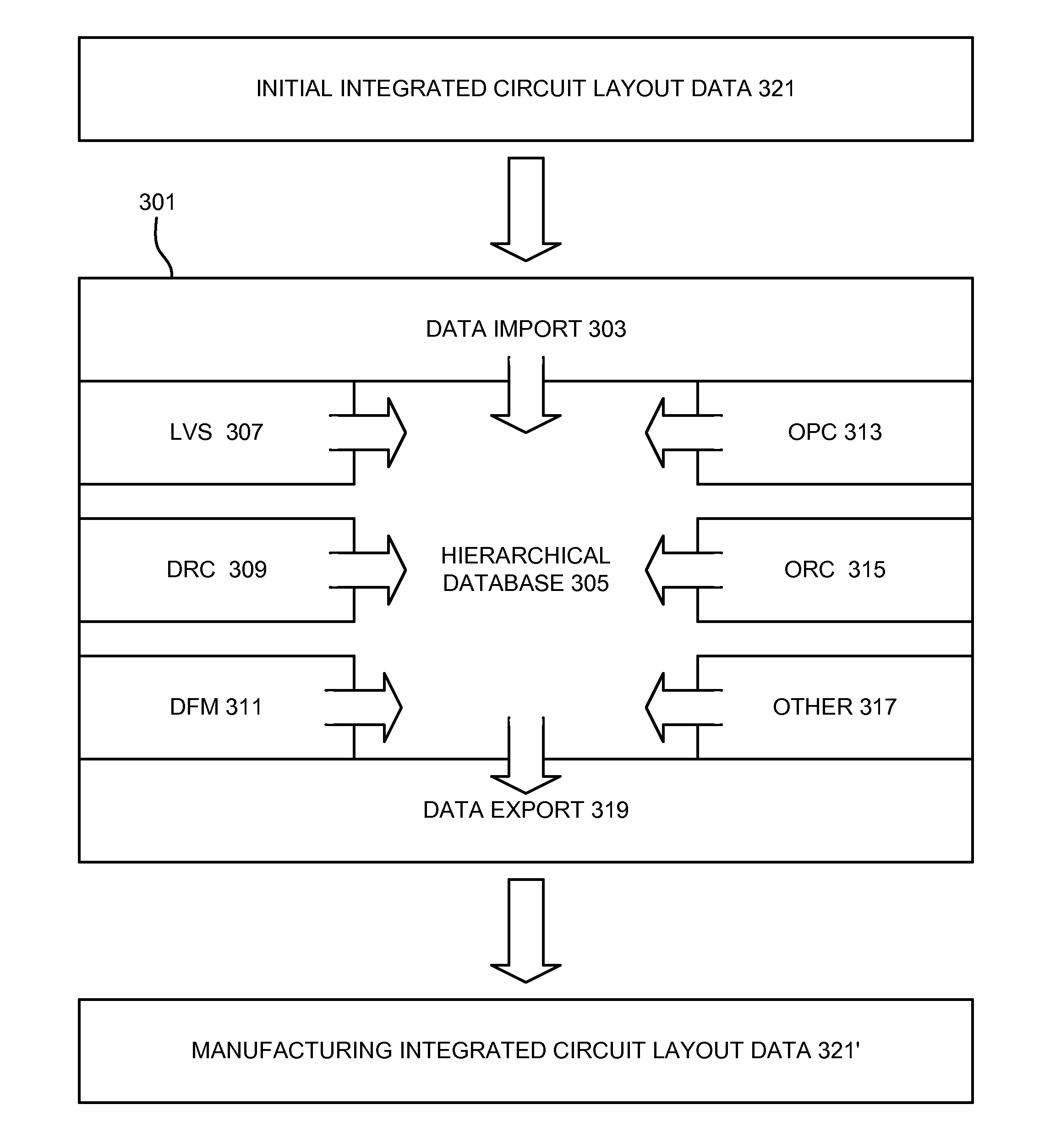
[0020]As will be discussed in more detail below, various embodiments of the invention relate to analog design-rule-check tools for creating and implementing models for various electronic design automation verification processes. With some examples of the invention, an analog design-rule-check tool can be incorporated into a larger electronic design automation verification tool. For still other examples of the invention, an analog design-rule-check tool can be configured as a separate, stand-alone tool. With both arrangements, however, an analog design-rule-check tool according to various embodiments of the invention may be implemented using computer-executable software instructions executable or executed by one or more programmable computing devices.

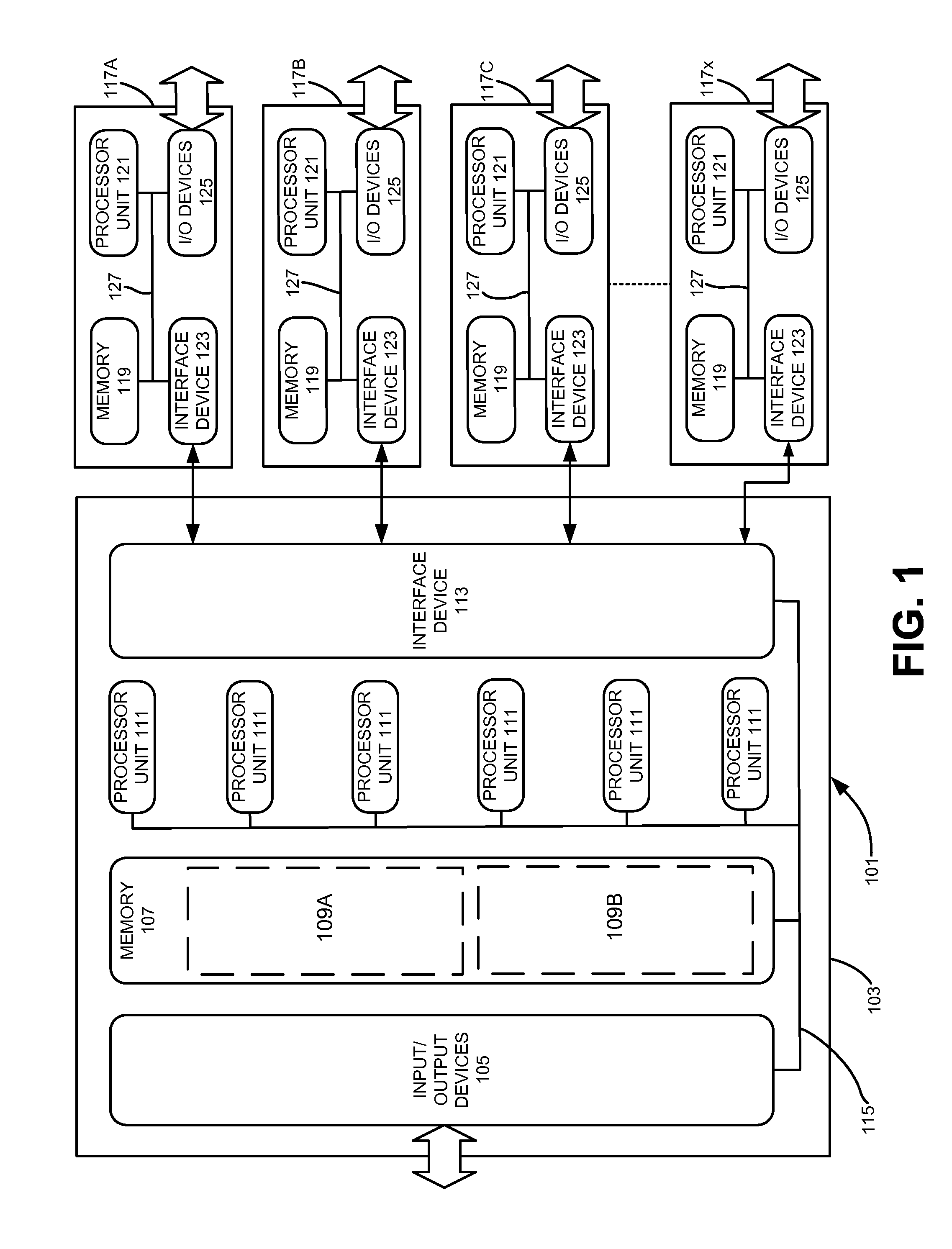
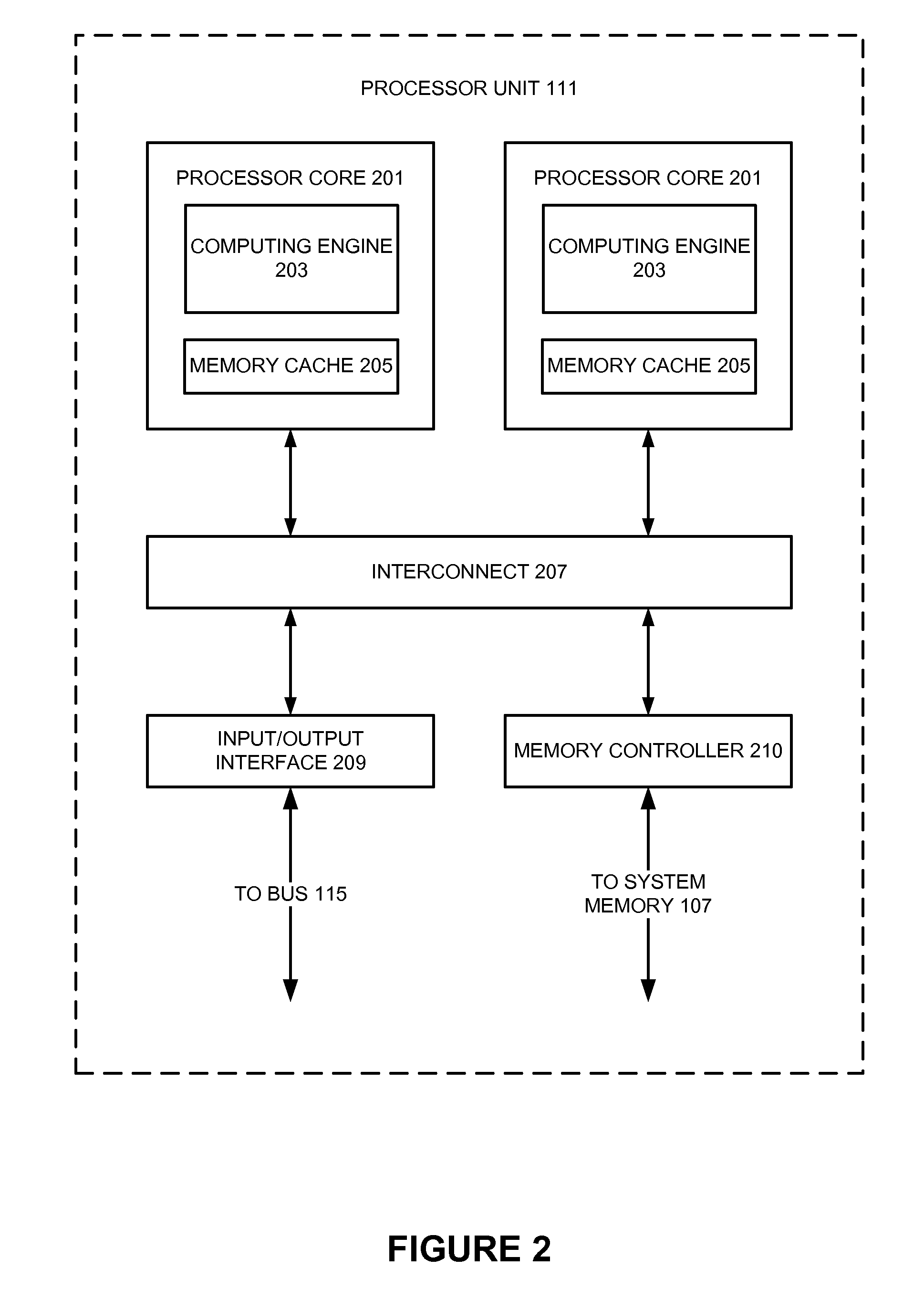
[0021]Because various embodiments of the invention may be implemented using software instructions, the components and operation of a generic programmable computer system on which various embodiments of the invention ...


PUM


Abstract

Techniques for efficiently determining whether an interconnect line has an impedance component value below a maximum specified value. A specified maximum impedance component value is used to limit the number of interconnect lines that are analyzed by a parasitic extraction analysis process. An analysis window is created based upon the characteristics of the interconnect lines and the specified maximum impedance component value. The size of the window corresponds to the minimum length of the interconnect line that would have the specified maximum impedance component value. Once the analysis window has been created, the interconnect lines are examined to determine if any of them reaches to (or beyond) the analysis window, whereby interconnect lines that exceed the specified maximum impedance component value can be identified. If there are any remaining interconnect lines that have not been determined to exceed the specified maximum impedance component value through the use of the analysis window, then the impedance component values of these remaining interconnect lines can be specifically determined using a parasitic extraction process.

Description

RELATED APPLICATIONS[0001]This application claims priority under 35 U.S.C. §119 to U.S. Provisional Patent Application No. 61 / 089,030, filed on Aug. 14, 2008, entitled “Electrostatic Damage Protection Circuitry Verification,” and naming Hazem Hegazy et al. as inventors, which application is incorporated entirely herein by reference. This application also claims priority under 35 U.S.C. §119 to U.S. Provisional Patent Application No. 61 / 089,050, filed on Aug. 14, 2008, entitled “Electrostatic Damage Protection Circuitry Verification,” and naming Fedor G. Pikus as inventor, which application is incorporated entirely herein by reference as well.FIELD OF THE INVENTION[0002]The present invention is directed to the verification of electrostatic damage protection circuitry verification in an integrated circuit design. Various implementations of the invention may be useful for verifying that one or more impedance components associated with an electrostatic damage protection circuit is below...

Claims


Application Information

Patent Timeline
Patent Type & Authority Applications(United States)
IPC IPC(8): G06F17/50
CPCG06F17/5081G06F30/398
Inventor PIKUS, FEDOR G.LU, ZIYANGGIBSON, PATRICK D.
Owner PIKUS FEDOR G
Learn More