
Organic light emitting display device and method of manufacturing the same

a technology of light-emitting display devices and organic materials, which is applied in the direction of static indicating devices, instruments, basic electric elements, etc., can solve the problems of brightness differences between the inner and outer surfaces of display devices, and achieve the effect of preventing non-uniform brightness

Inactive Publication Date: 2010-07-29
SAMSUNG DISPLAY CO LTD
View PDF5 Cites 26 Cited by
  • Summary
  • Abstract
  • Description
  • Claims
  • Application Information

AI Technical Summary

Benefits of technology

[0012]Therefore, it is an object of the present invention to provide an organic light emitting display device that prevents non-uniformity in brightness and after-images, and a method of manufacturing the same.
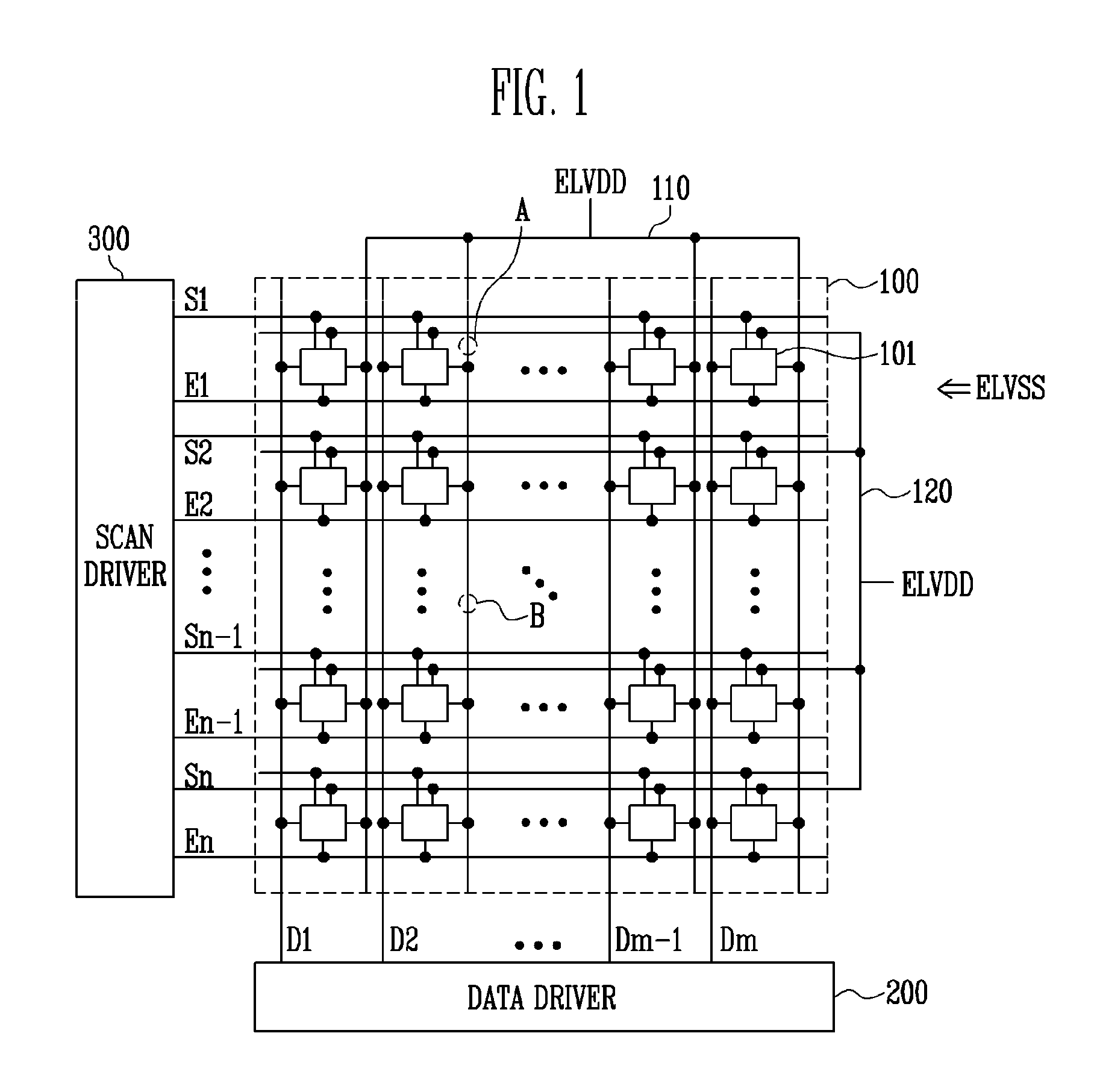
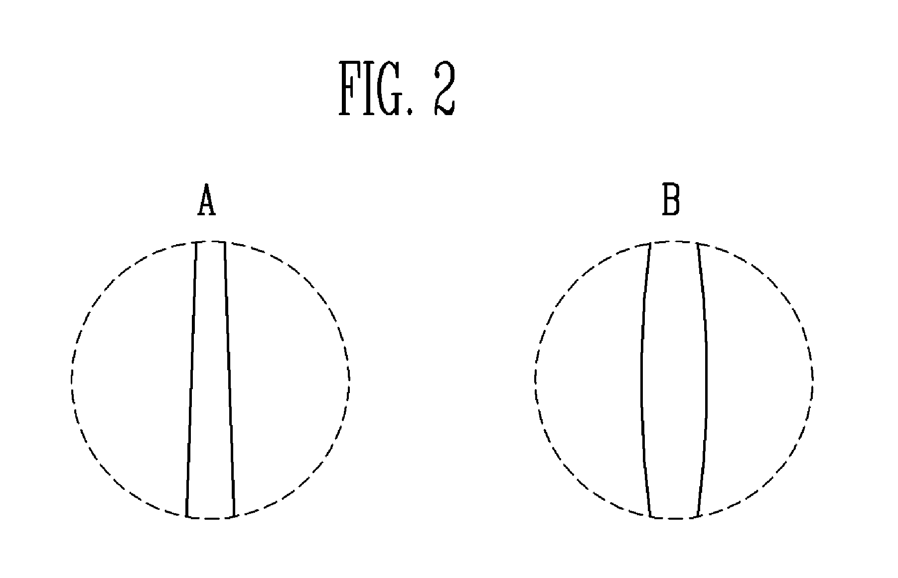
[0016]According to another aspect of the present invention, the lines to which the first power is transferred are formed in a mesh type and the width of the lines is controlled, making it possible to reduce the drop in the voltage from the first power supply, and also the difference between the magnitude of the drop in the voltage from the first power supply and the magnitude of the drop in the voltage from the second power supply is reduced, making it possible to achieve uniform brightness.
[0017]According to another aspect of the present invention, the deterioration of the organic light emitting diode is compensated, making it possible to reduce after-images.

Problems solved by technology

Therefore, a problem arises in that brightness difference occurs between the inner and the outer surfaces of the display device.
Also, the respective organic light emitting diodes deteriorate over time, which causes unnecessary current to flow into the organic light emitting diodes, thereby forming after-images, etc.

Method used


Image

  • Organic light emitting display device and method of manufacturing the same
  • Organic light emitting display device and method of manufacturing the same
  • Organic light emitting display device and method of manufacturing the same

Examples


Embodiment Construction

[0025]Reference will now be made in detail to the present embodiments of the present invention, examples of which are illustrated in the accompanying drawings. The embodiments are described below in order to explain the present invention by referring to the figures.

[0026]Here, when a first element is described as being coupled to a second element, the first element may be not be only directly coupled to the second element but may also be indirectly coupled to the second element via a third element. Moreover, it is to be understood that where is stated herein that one film or layer is “formed on” or “disposed on” a second layer or film, the first layer or film may be formed or disposed directly on the second layer or film or there may be intervening layers or films between the first layer or film and the second layer or film. Further, as used herein, the term “formed on” is used with the same meaning as “located on” or “disposed on” and is not meant to be limiting regarding any parti...


PUM


Abstract

An organic light emitting display device includes a pixel unit that displays an image corresponding to an amount of driving current flowing from a first power supply to a second power supply, wherein the pixel unit includes a pixel that is formed at an intersection portion of a scan line transferring a scan signal and a data line transferring a data signal. The pixel electrode further includes organic light emitting diodes emitting light according to the driving current, and controlling the magnitude of the driving current by controlling a voltage of the data signal corresponding to voltages from the first power supply and the second power supply and a voltage formed on the organic light emitting diode; a first wire transferring the first power to the pixel in a first direction; and a second wire transferring the first power to the pixel in a second direction, wherein the first wire and the second wire are formed to have a thickness thicker in the mid-portion of the pixel unit and is thinner in an outer-portion of the pixel unit, and a method of manufacturing the same.

Description

CROSS-REFERENCE TO RELATED APPLICATION[0001]This application claims priority to and the benefit of Korean Patent Application No. 10-2009-0006905, filed on Jan. 29, 2009, in the Korean Intellectual Property Office, the entire content of which is incorporated herein by reference.BACKGROUND OF THE INVENTION[0002]1. Field of the Invention[0003]An aspect of the present invention relates to an organic light emitting display device and a method of manufacturing the same, and more particularly, to an organic light emitting display device that improves image quality by reducing a difference of voltage drop in power wires, and a method of manufacturing the same.[0004]2. Description of the Related Art[0005]Recently, various flat panel display devices having reduced weight and volume as compared to cathode ray tubes have been developed. Amongst the various types of flat panel display devices, there are liquid crystal display (LCD) devices, field emission display (FED) devices, plasma display pa...

Claims


Application Information

Patent Timeline
Patent Type & Authority Applications(United States)
IPC IPC(8): G09G5/00H01L21/28
CPCG09G3/3233G09G2300/0819H01L27/3276G09G2320/043G09G2320/045G09G2300/0852H10K59/131H01L23/53214H01L2924/01042H10K59/122
Inventor KIM, YANG-WAN
Owner SAMSUNG DISPLAY CO LTD
Learn More