Solid-state imaging device, imaging apparatus, and signal reading method of solid-state imaging device

a solid-state imaging and signal reading technology, applied in the direction of radio frequency controlled devices, television system scanning details, television systems, etc., can solve the problems of inability to achieve a wide dynamic range, inability to increase capacitance, image quality degradation, etc., to increase reliability and image quality, the effect of high sensitivity

Inactive Publication Date: 2010-07-29
FUJIFILM CORP
View PDF1 Cites 5 Cited by
  • Summary
  • Abstract
  • Description
  • Claims
  • Application Information

AI Technical Summary

Benefits of technology

[0011]The invention can provide a solid-state imaging device capable of attaining both of high sensitivity and a wide dynamic range and increasing the reliability and the image quality, a signal reading method of the solid-state imaging device, and an imaging apparatus having the solid-state imaging device.

Problems solved by technology

As a result, noise or the like that enters each FD from its neighborhood varies from one line to another to cause image quality degradation.
Therefore, to increase the sensitivity, it is necessary to reduce the capacitance C. However, if the capacitance C is reduced, the FD is saturated sooner and hence a wide dynamic range cannot be attained.
Conversely, if priority is given to increase of the dynamic range, the capacitance needs to be increased and hence high sensitivity cannot be attained.
That is, in the solid-state imaging device disclosed in US-A-2007-0221823, it is difficult to attain both of high sensitivity and a wide dynamic range.

Method used


Image

  • Solid-state imaging device, imaging apparatus, and signal reading method of solid-state imaging device
  • Solid-state imaging device, imaging apparatus, and signal reading method of solid-state imaging device
  • Solid-state imaging device, imaging apparatus, and signal reading method of solid-state imaging device

Examples


Embodiment Construction

[0016]A solid-state imaging device according to an embodiment of the present invention will be hereinafter described with reference to the drawings. This solid-state imaging device is for use in an imaging apparatus such as a digital camera, a digital video camera, or an electronic endoscope.

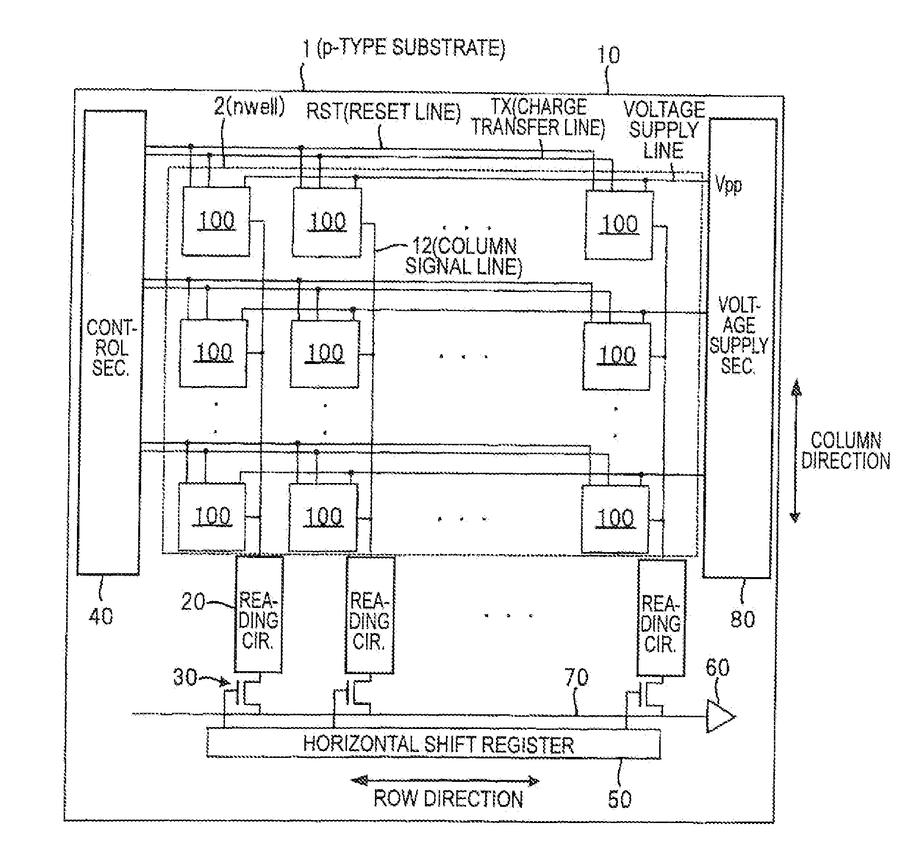
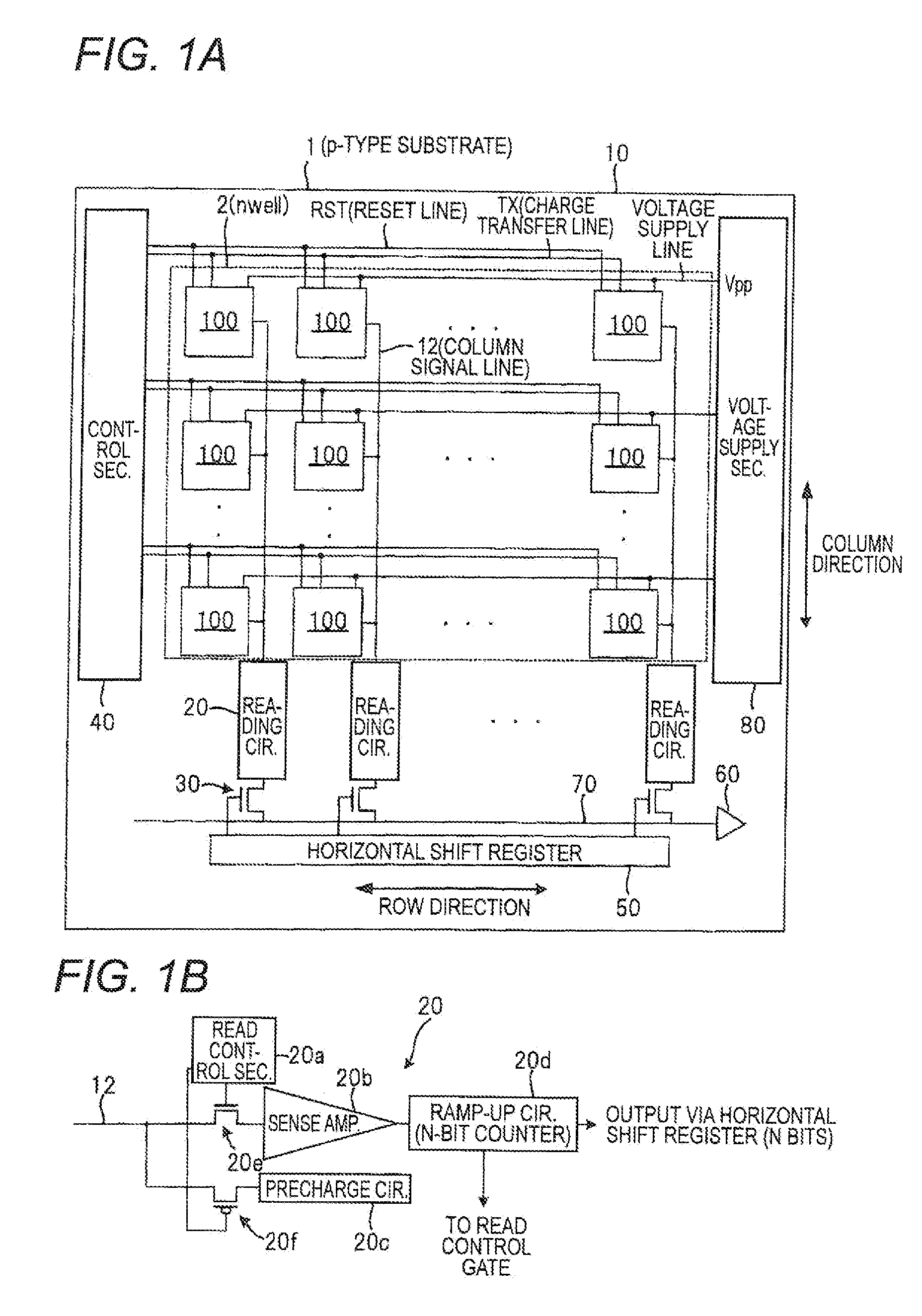
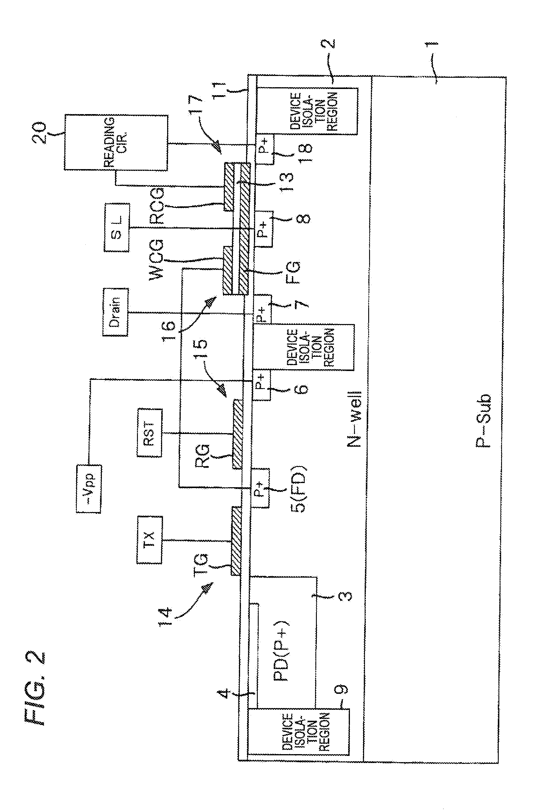
[0017]FIG. 1A is a schematic plan view showing a general configuration of the solid-state imaging device according to the embodiment of the invention, and FIG. 1B is a block diagram of each reading circuit. FIG. 2 is a schematic sectional view showing a general configuration of each of pixel portions shown in FIG. 1A. FIG. 3 is an equivalent circuit diagram of the pixel portion of FIG. 2.

[0018]The solid-state imaging device 10 is provided with plural pixel portions 100 which are arranged in the same plane in a row direction and a column direction that is perpendicular to the row direction so as to form an array (in this example, a square lattice).

[0019]Each pixel portion 100 is provided with a p...


PUM


Abstract

A solid-state imaging device includes a plurality of pixel portions, each of the pixel portions includes: a semiconductor photoelectric conversion portion for generating holes according to an amount of incident light and storing the generated holes; a semiconductor floating diffusion layer for converting the holes generated in the photoelectric conversion portion into a voltage corresponding to an amount of the generated holes; and a transistor having a gate electrode which is connected to an output of the floating diffusion layer and an electron storage portion which is disposed under the gate electrode and an amount of electrons stored in which varies depending on a voltage applied to the gate electrode, and the solid-state imaging device further includes: a reading circuit as defined herein.

Description

CROSS-REFERENCE TO RELATED APPLICATIONS[0001]This application claims the benefit of Japanese Patent Application JP 2009-014231, filed Jan. 26, 2009, the entire content of which is hereby incorporated by reference, the same as if set forth at length.FIELD OF THE INVENTION[0002]The present invention relates to a solid-state imaging device, an imaging apparatus, and a signal reading method of a solid-state imaging device.BACKGROUND OF THE INVENTION[0003]US-A-2007-0221823 proposes a CMOS solid-state imaging device in which a global shutter is realized in such a manner that charges generated in all photodiodes (PDs) are transferred to respective floating diffusion layers (FDs) and voltage signals corresponding to potential variations of the FDs are read out while the timing is shifted on a line-by-line basis.[0004]However, in this solid-state imaging device, since voltage signals are read out while the timing is shifted on a line-by-line basis, the standby time to reading-out of voltage ...

Claims


Application Information

Patent Timeline
Patent Type & Authority Applications(United States)
IPC IPC(8): H04N5/335H01L27/146H04N5/355H04N5/369H04N5/374H04N5/3745
CPCH01L27/14609H04N5/378H04N5/374H04N25/76H04N25/75
Inventor SHIZUKUISHI, MAKOTO
Owner FUJIFILM CORP
Why Eureka
Try Eureka