
Flat panel display apparatus and method of manufacturing the same

a technology of display apparatus and flat panel, which is applied in the direction of electrical apparatus, semiconductor devices, instruments, etc., can solve the problems of complex pattern transfer operations, increased cost of fabricating masks, and complicated overall fabricating process, so as to achieve excellent display quality and less patterning operations

Active Publication Date: 2010-08-05
SAMSUNG DISPLAY CO LTD
View PDF7 Cites 136 Cited by
  • Summary
  • Abstract
  • Description
  • Claims
  • Application Information

AI Technical Summary

Benefits of technology

[0009]Aspects of the present invention provide a flat panel display apparatus having excellent display quality and that can be manufactured with less patterning operations using a mask, and a method of manufacturing the same.

Problems solved by technology

In the process of transferring a pattern by using the mask as described above, it is necessary to prepare the mask having a required pattern, and thus costs for fabricating the mask increase as more operations are performed using the mask.
Furthermore, complex operations described above are required to transfer a pattern by using the mask.
Thus, the overall fabricating process becomes complicated, and time and cost required for a fabrication operation increase.

Method used


Image

  • Flat panel display apparatus and method of manufacturing the same
  • Flat panel display apparatus and method of manufacturing the same
  • Flat panel display apparatus and method of manufacturing the same

Examples


Embodiment Construction

[0026]Reference will now be made in detail to the present embodiments of the present invention, examples of which are illustrated in the accompanying drawings, wherein like reference numerals refer to the like elements throughout. The embodiments are described below in order to explain the present invention by referring to the figures.

[0027]As referred to herein, when a first element is said to be disposed or formed “on” a second element, the first element can directly contact the second element, or can be separated from the second element by one or more other elements located therebetween. In contrast, when an element is referred to as being disposed or formed “directly on” another element, there are no intervening elements present.

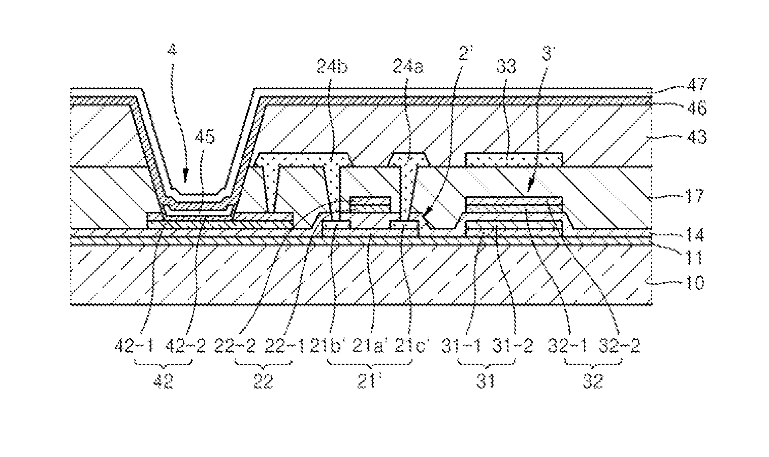
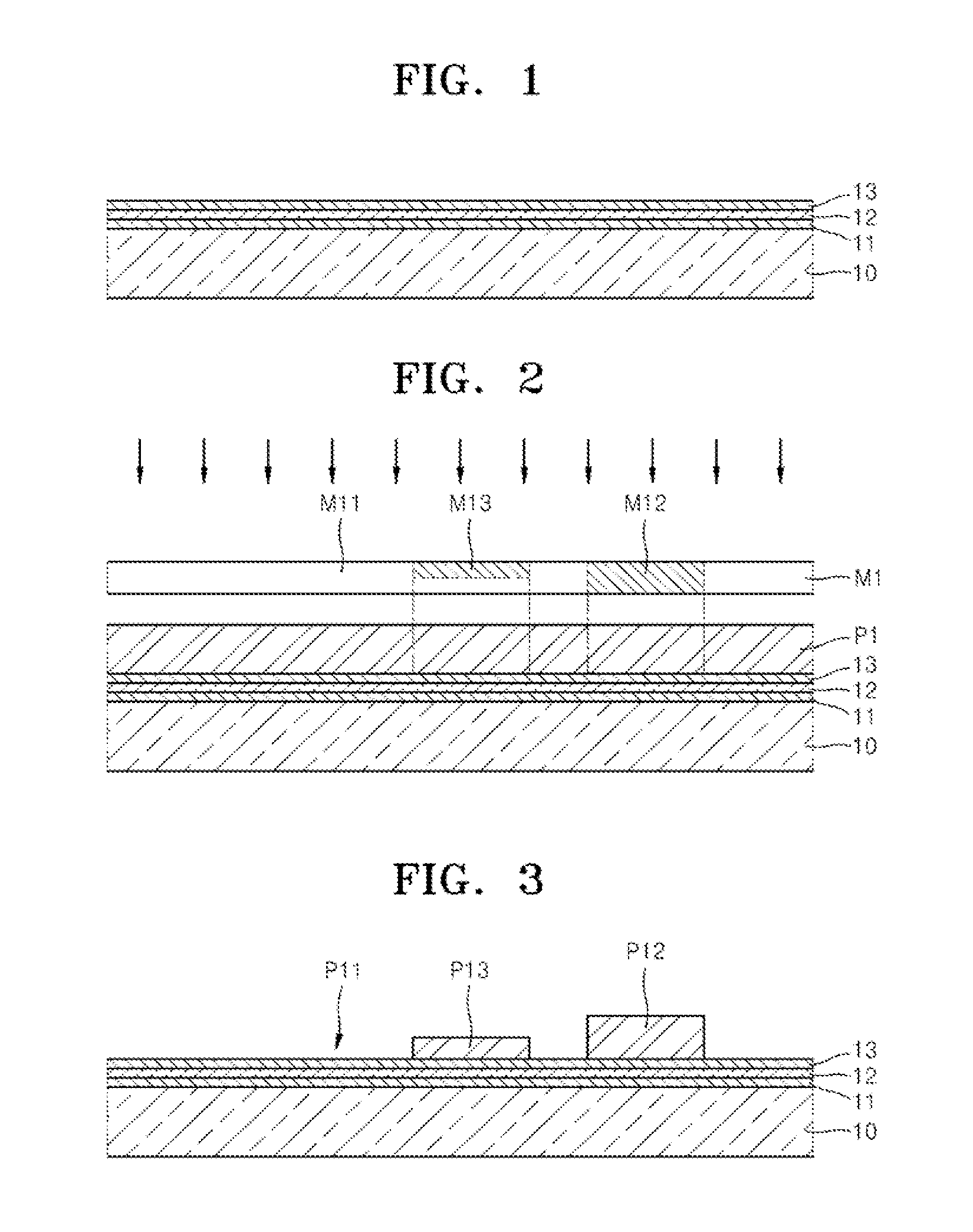
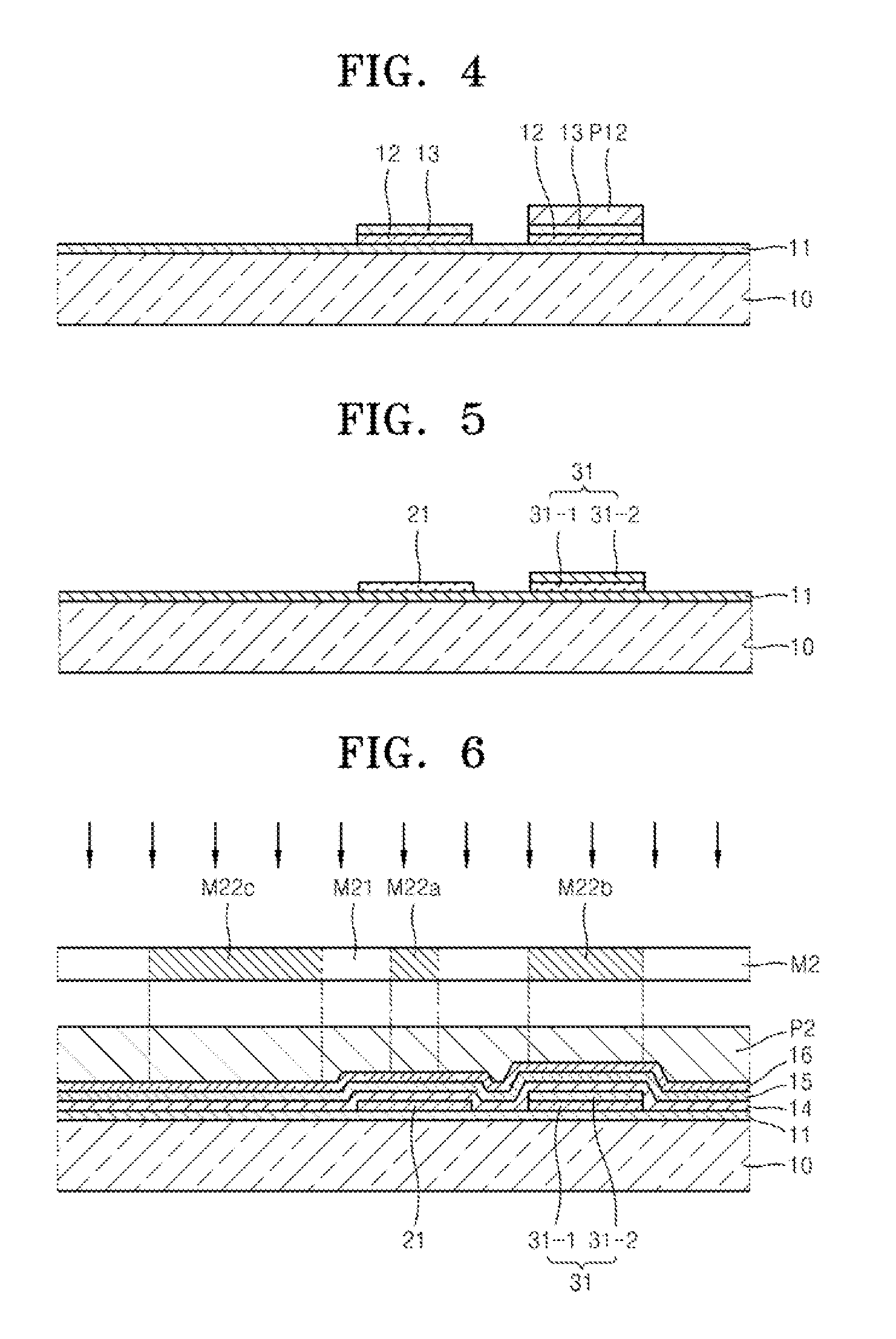
[0028]First, referring to FIGS. 1 through 16, a flat panel display apparatus according to an embodiment of the present invention will be described.

[0029]FIGS. 1 through 15 are sectional views roughly showing a method of manufacturing an organic light emi...


PUM


Abstract

A flat panel display apparatus that can be manufactured with less patterning operations using a mask, and a method of manufacturing the same, the flat panel display apparatus including a substrate; an active layer of a thin film transistor (TFT); a first bottom electrode and a first top electrode of a capacitor; a first insulation layer formed on the substrate; a gate bottom electrode and a gate top electrode corresponding to the channel region; a second bottom electrode and a second top electrode of the capacitor; a pixel bottom electrode and a pixel top electrode; a second insulation layer formed on the gate electrode, the second electrode of the capacitor, and the pixel top electrode; and a source electrode and a drain electrode formed on the second insulation layer.

Description

CROSS-REFERENCE TO RELATED APPLICATION[0001]This application claims the benefit of Korean Application No. 10-2009-0007385, filed Jan. 30, 2009, in the Korean Intellectual Property Office, the disclosure of which is incorporated herein by reference.BACKGROUND OF THE INVENTION[0002]1. Field of the Invention[0003]Aspects of the present invention relate to a flat panel display apparatus and a method of manufacturing the same, and more particularly, to a flat panel display apparatus having increased display quality and that can be manufactured simply, and a method of manufacturing the same.[0004]2. Description of the Related Art[0005]Flat panel display apparatuses, such as organic light emitting diode (OLED) apparatuses, liquid crystal display (LCD) apparatuses, and other similar display apparatuses, are fabricated on a substrate on which a pattern including a thin film transistor (TFT), a capacitor, and wiring connecting the TFT and the capacitor is formed.[0006]Generally, a fine struct...

Claims


Application Information

Patent Timeline
IPC IPC(8): H01L33/00H01L21/28
CPCH01L27/3244H01L27/3248H01L27/3262H01L2227/323H01L51/5206H01L51/56H01L27/3265H01L27/1255H01L29/4908H10K59/123H10K59/1216H10K59/1213H10K59/1201H10K59/80517G02F1/136G02F1/1343H10K50/81
Inventor YEO, JONG-MONO, DAE-HYUNKWON, DO-HYUNIM, CHOONG-YOULJO, SOO-BEONDOH, SUNG-WONLEE, IL-JEONGYU, CHEOL-HO
Owner SAMSUNG DISPLAY CO LTD
Features
  • Generate Ideas
  • Intellectual Property
  • Life Sciences
  • Materials
  • Tech Scout
  • Unparalleled Data Quality
  • Higher Quality Content
  • 60% Fewer Hallucinations
Learn More