Organic light emitting display device

a light-emitting display and organic technology, applied in the direction of solid-state devices, semiconductor devices, thermoelectric devices, etc., can solve the problems of easy settling, easy settling, and complicated process of inkjet printing, and achieve the effect of reducing or avoiding external appearance defects

Active Publication Date: 2010-08-19
SAMSUNG DISPLAY CO LTD
View PDF4 Cites 39 Cited by
  • Summary
  • Abstract
  • Description
  • Claims
  • Application Information

AI Technical Summary

Benefits of technology

[0012]The organic light emitting display device according to exemplary embodiments of the present invention includes a plurality of spacers that are arranged in a dot configuration or arrangement along the outer sides of the light emitting regions, and have cross-sections with an upper portion smaller than a lower portion. The shadow masks that selectively deposit an organic material are evenly supported in the light emitting regions at an interval (e.g., a predetermined interval) by the spacers arranged in a dot configuration, such that the organic light emitting layer can be formed in an accurate pattern (e.g., shape). Also, the spacers form dot or point contacts with the sealing substrate and maintain an interval between the substrate and the sealing substrate, such that the contact areas with the sealing substrate are minimized or reduced, thereby and reducing or avoiding external appearance defects due to stains.

Problems solved by technology

However, the inkjet printing method is a complicated process, because a surface of a substrate should be planarized so that an organic material can be printed, and organic layers are limited to particular materials.
However, due to drooping of the mask, it is not easy to deposit the organic materials in an exact pattern (e.g., shape), and the method is not applicable to a large-sized substrate.
Also, stains may be formed due to contact with the mask, thereby causing a defective external appearance.

Method used


Image

  • Organic light emitting display device
  • Organic light emitting display device
  • Organic light emitting display device

Examples


Embodiment Construction

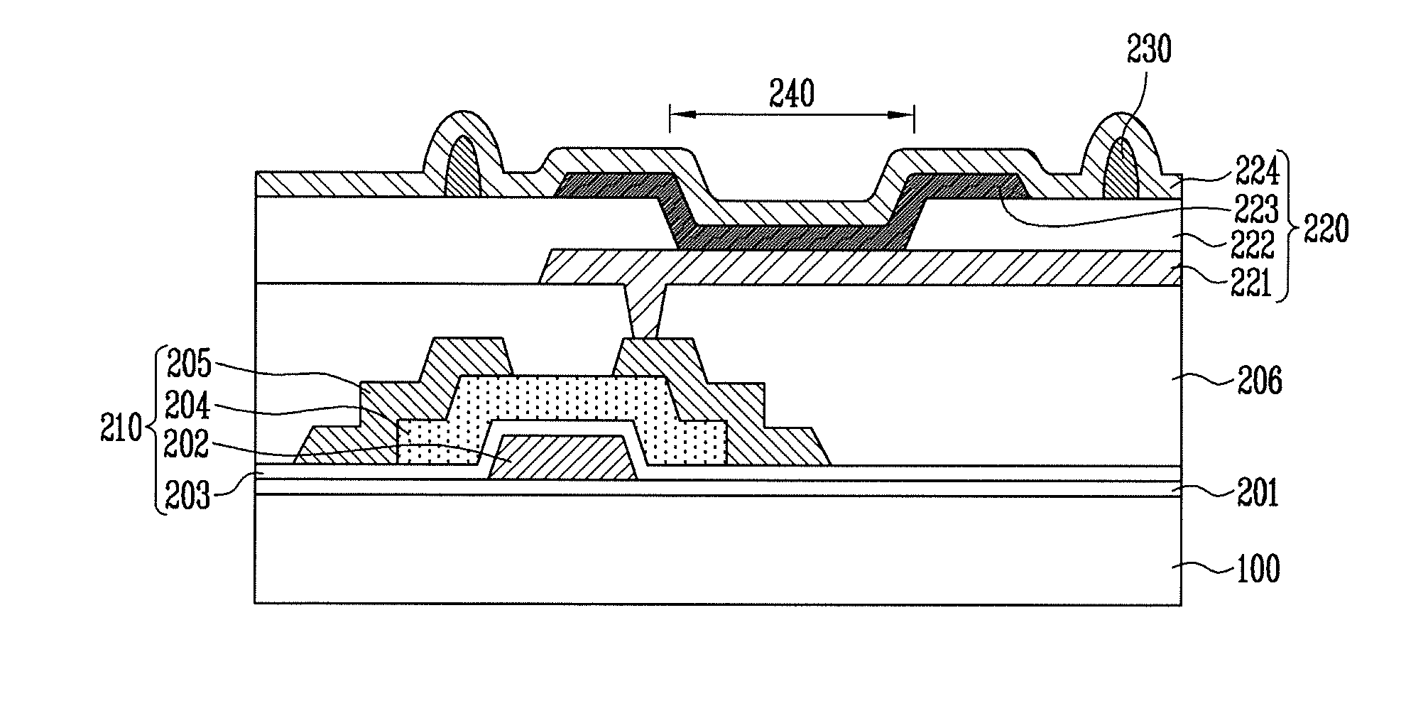
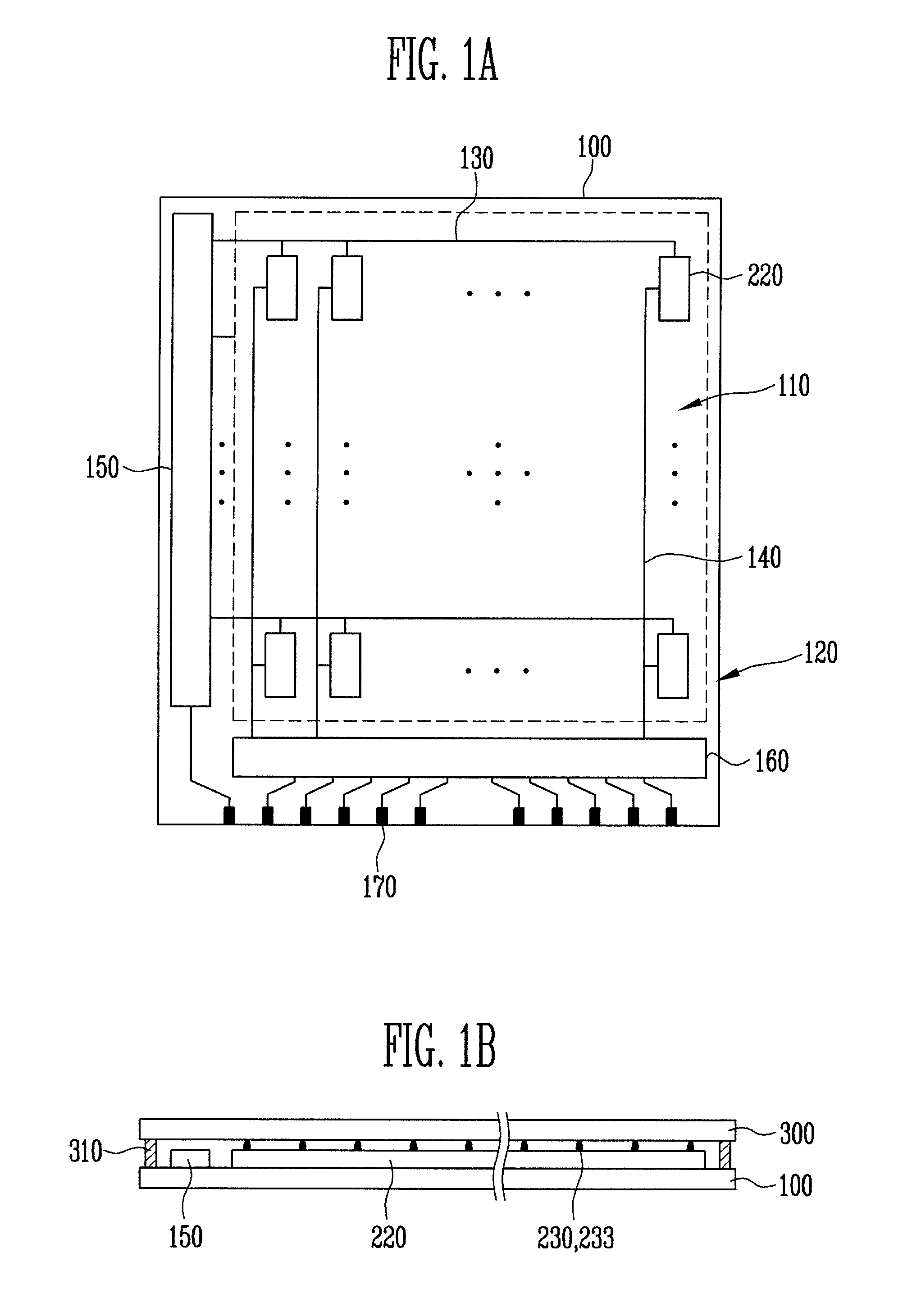
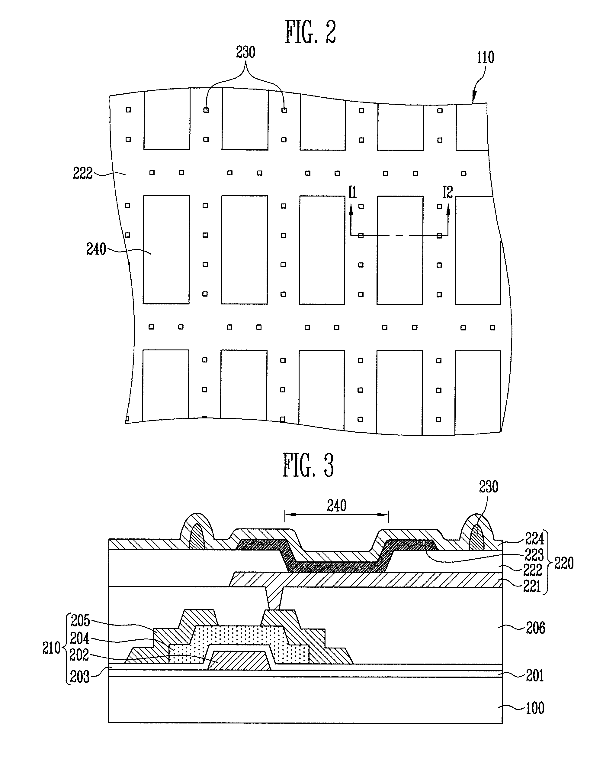
[0020]In the following detailed description, only certain exemplary embodiments of the present invention have been shown and described by way of illustration. As those skilled in the art will recognize, the described embodiments may be modified in various different ways without departing from the spirit or scope of the present invention. Accordingly, the drawings and description are to be regarded as illustrative in nature and not restrictive. In addition, when an element is referred to as being “on” another element, it may be directly on the another element, or may be indirectly on the another element, with one or more elements interposed therebetween. Also, when an element is referred to as being “connected to” another element, it may be directly connected to the another element, or may be indirectly connected to the another element, with one or more elements connected therebetween. Hereinafter, like reference numerals refer to like elements.

[0021]Hereinafter, exemplary embodiment...


PUM


Abstract

An organic light emitting display device includes: a first substrate; a plurality of organic light emitting diodes on the first substrate; a plurality of spacers spaced apart from each other on sides of light emitting regions corresponding to the plurality of organic light emitting diodes; and a second substrate facing the first substrate and spaced apart from the first substrate at an interval by the plurality of spacers.

Description

CROSS-REFERENCE TO RELATED APPLICATIONS[0001]This application claims priority to and the benefit of Korean Patent Application No. 10-2009-0012312, filed on Feb. 16, 2009, in the Korean Intellectual Property Office, the entire content of which is incorporated herein by reference.BACKGROUND[0002]1. Field of the Invention[0003]The present invention relates to an organic light emitting display device, and more particularly, to an organic light emitting display device having spacers.[0004]2. Description of Related Art[0005]An organic light emitting display device emits light by itself and has excellent properties with respect to viewing angles, contrast, response times, and power consumption, among other properties, when compared to, for example, a liquid crystal display device (LCD).[0006]An organic light emitting diode in a pixel of the organic light emitting display device includes an anode electrode, a cathode electrode and an organic light emitting layer, and emits light in accordan...

Claims


Application Information

Patent Timeline
Patent Type & Authority Applications(United States)
IPC IPC(8): H01L51/50H01L33/00
CPCH01L51/525H01L51/5237H10K59/122H10K50/8428H01L2924/13069H10K50/84
Inventor KIM, TAE-GON
Owner SAMSUNG DISPLAY CO LTD
Why Eureka
Try Eureka