Non-volatile semiconductor storage device and method of manufacturing the same

a non-volatile, semiconductor technology, applied in semiconductor devices, electrical equipment, instruments, etc., can solve the problems of increasing the cost and technology of lithography process, increasing the cost of lithography process, and achieving the physical limit of lithography

Active Publication Date: 2010-08-19
KIOXIA CORP
View PDF18 Cites 950 Cited by
  • Summary
  • Abstract
  • Description
  • Claims
  • Application Information

AI Technical Summary

Problems solved by technology

Although the size of one element is ordinarily reduced (miniaturized) to increase the storage capacity of a memory, this becomes recently difficult from a viewpoint of cost and technology.
Although a photolithography technology must be improved for miniaturization, a cost necessary for a lithography process is more and more increased.
Further, even if miniaturization has been achieved, it is predicted that a withstanding voltage between elements and the like reach a physical limit unless a drive voltage and the like are scaled.
That is, there is a high possibility that a device becomes difficult to operate.
The memory cells are three-dimensionally formed by repeating the above processes a plurality of times. However, a problem arises in that the memory gate insulation layers are removed by etching due to the diluted fluorinated acid process.

Method used


Image

  • Non-volatile semiconductor storage device and method of manufacturing the same
  • Non-volatile semiconductor storage device and method of manufacturing the same
  • Non-volatile semiconductor storage device and method of manufacturing the same

Examples


first embodiment

[0060](Arrangement of Non-Volatile Semiconductor Storage Device 100 according to First Embodiment)

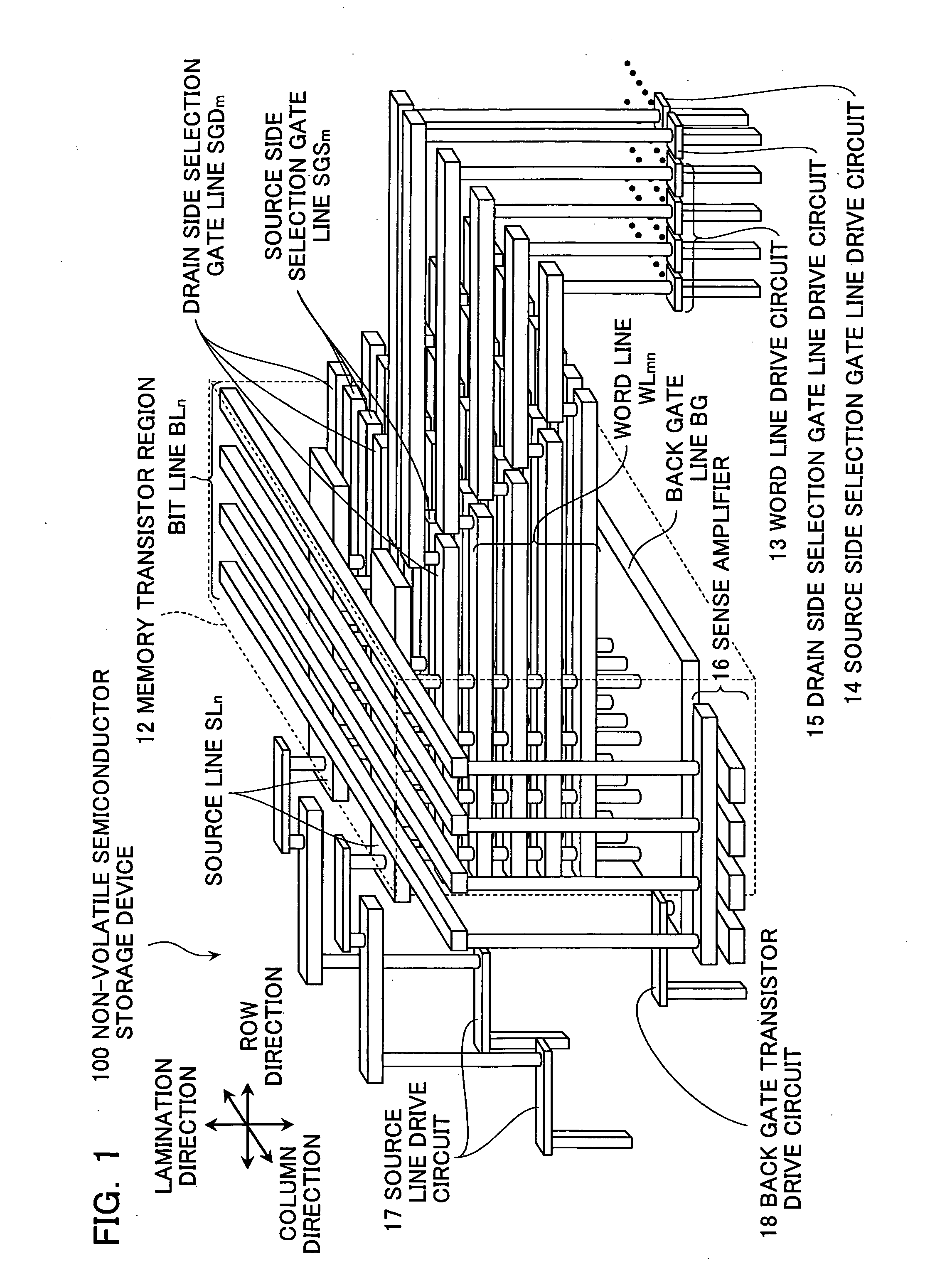
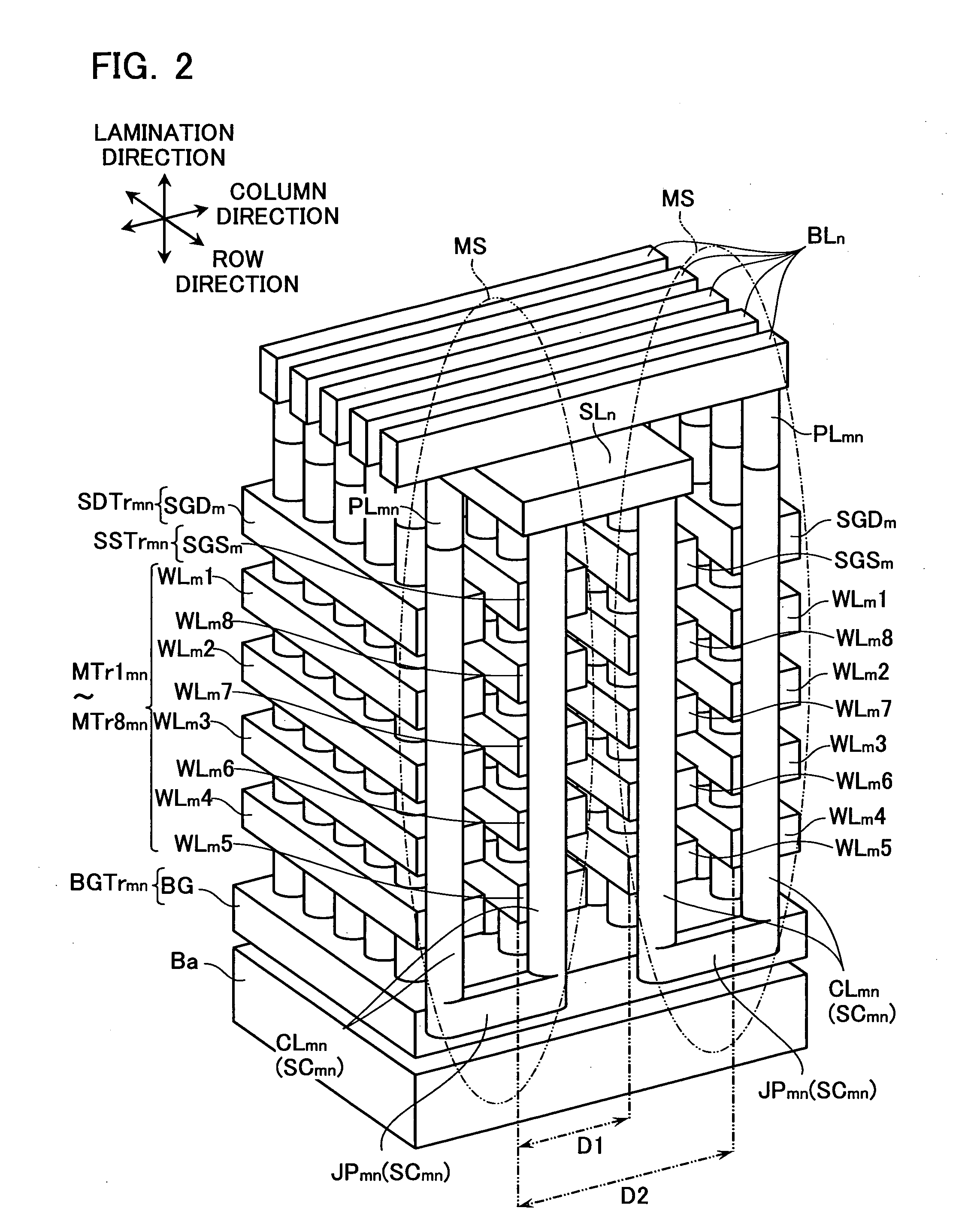
[0061]FIG. 1 shows a schematic view of a non-volatile semiconductor storage device 100 according to a first embodiment of the present invention. As shown in FIG. 1, the non-volatile semiconductor storage device 100 according to the first embodiment mainly has a memory transistor region 12, a word line drive circuit 13, a source side selection gate line (SGSm) drive circuit 14, a drain side selection gate line (SGDm) drive circuit 15, a sense amplifier 16, a source line drive circuit 17, and a back gate transistor drive circuit 18. The memory transistor region 12 has memory transistors for storing data. The word line drive circuit 13 controls a voltage applied to the word line WL. The source side selection gate line (SGSm) drive circuit 14 controls a voltage applied to the source side selection gate line SGS. The drain side selection gate line (SGDm) drive circuit 15 controls a voltage a...

second embodiment

[0176](Arrangement of Non-Volatile Semiconductor Storage Device according to Second Embodiment)

[0177]Next, an arrangement of a non-volatile semiconductor storage device according to a second embodiment will be explained referring to FIGS. 47 and 48. FIG. 47 is a schematic perspective view of a part of a memory transistor region of the non-volatile semiconductor storage device according to the second embodiment, and FIG. 48 is a sectional view of the memory transistor region.

[0178]As shown in FIGS. 47 and 48, a memory transistor layer 30a and a select gate transistor layer 40a in the non-volatile semiconductor storage device according to the second embodiment are arranged different from those of the first embodiment.

[0179]In the memory transistor layer 30a and the select gate transistor layer 40a, a source side selection gate line SGSm′ (source side conductive layer 421) and word lines WLm1′ to WLm8′ (first to eighth word line conductive layers 321a to 321h) are arranged different fr...

third embodiment

[0188](Arrangement of Non-Volatile Semiconductor Storage Device according to Third Embodiment)

[0189]Next, an arrangement of a non-volatile semiconductor storage device according to a third embodiment will be explained referring to FIGS. 49 and 50. FIG. 49 is a schematic perspective view of a part of a memory transistor region of the non-volatile semiconductor storage device according to the third embodiment, and FIG. 50 is a sectional view of the memory transistor region.

[0190]As shown in FIGS. 49 and 50, in the non-volatile semiconductor storage device according to the third embodiment, an arrangement of a back gate line BG′ (back gate transistor layer 20a) is different from the first embodiment. The back gate line BG′ (back gate transistor layer 20a) according to the third embodiment has a first back gate line BG1′ (first back gate conductive layer 22a) and a second back gate line BG2′ (second back gate conductive layer 22b) formed on the first back gate line BG1′ (first back gate...


PUM


Abstract

A non-volatile semiconductor storage device has a plurality of memory strings to each of which a plurality of electrically rewritable memory cells are connected in series. Each of the memory strings includes first semiconductor layers each having a pair of columnar portions extending in a vertical direction with respect to a substrate and a coupling portion formed to couple the lower ends of the pair of columnar portions; a charge storage layer formed to surround the side surfaces of the columnar portions; and first conductive layers formed to surround the side surfaces of the columnar portions and the charge storage layer. The first conductive layers functions as gate electrodes of the memory cells.

Description

TECHNICAL FIELD[0001]The present invention relates to an electrically rewritable non-volatile semiconductor storage device and to a method of manufacturing the same.BACKGROUND ART[0002]Conventionally, LSIs are formed by integrating elements in a two-dimensional plane on a silicon substrate. Although the size of one element is ordinarily reduced (miniaturized) to increase the storage capacity of a memory, this becomes recently difficult from a viewpoint of cost and technology. Although a photolithography technology must be improved for miniaturization, a cost necessary for a lithography process is more and more increased. Further, even if miniaturization has been achieved, it is predicted that a withstanding voltage between elements and the like reach a physical limit unless a drive voltage and the like are scaled. That is, there is a high possibility that a device becomes difficult to operate.[0003]To cope with the above problem, recently, a lot of semiconductor storage devices are ...

Claims


Application Information

Patent Timeline
Patent Type & Authority Applications(United States)
IPC IPC(8): H01L29/792H01L21/336
CPCG11C16/0483H01L27/11551H01L27/11556H01L27/11575H01L27/11578H01L27/1052H01L27/11582H01L27/11573H10B43/50H10B43/40H10B41/27H10B43/27H01L27/0688H10B99/00H10B41/20H10B43/20H01L29/513
Inventor FUKUZUMI, YOSHIAKIKATSUMATA, RYOTAKIDOH, MASARUKITO, MASARUTANAKA, HIROYASUKOMORI, YOSUKEISHIDUKI, MEGUMIAOCHI, HIDEAKI
Owner KIOXIA CORP
Why Eureka
Try Eureka