All optical processing circuit for conflict resolution and switch configuration in a 2x2 optical node

a technology of conflict resolution and optical processing circuit, which is applied in logic circuits using specific components, pulse techniques, instruments, etc., can solve the problems of slowing the throughput of switches, and achieve the effect of simple arrangement and minimise the time for signals to propagate through the circui

Active Publication Date: 2010-08-19
TELEFON AB LM ERICSSON (PUBL)
View PDF1 Cites 11 Cited by
  • Summary
  • Abstract
  • Description
  • Claims
  • Application Information

AI Technical Summary

Benefits of technology

[0015]The destination address signals AH and AL and packet identifier signal PIH may comprise respective one-bit signals. Also the CRC and SCG signals may comprise one bit signals which are suitable for controlling a 2×2 optical switched node. This eases the implementation of an optical logic circuit.
[0024]This arrangement of logic gates provide an especially simple arrangement with a low number of optical components which minimises the time for the signals to propagate through the circuit.

Problems solved by technology

A problem arises if two signals arrive, at respective input ports, at the same time, and both want to be sent to the same output port.
This electronic domain processing and the need to convert from the optical to the electronic domain slows the throughput of the switch and has been found to be limiting in the maximum rate at which signals can be passed

Method used


Image

  • All optical processing circuit for conflict resolution and switch configuration in a 2x2 optical node
  • All optical processing circuit for conflict resolution and switch configuration in a 2x2 optical node
  • All optical processing circuit for conflict resolution and switch configuration in a 2x2 optical node

Examples


Embodiment Construction

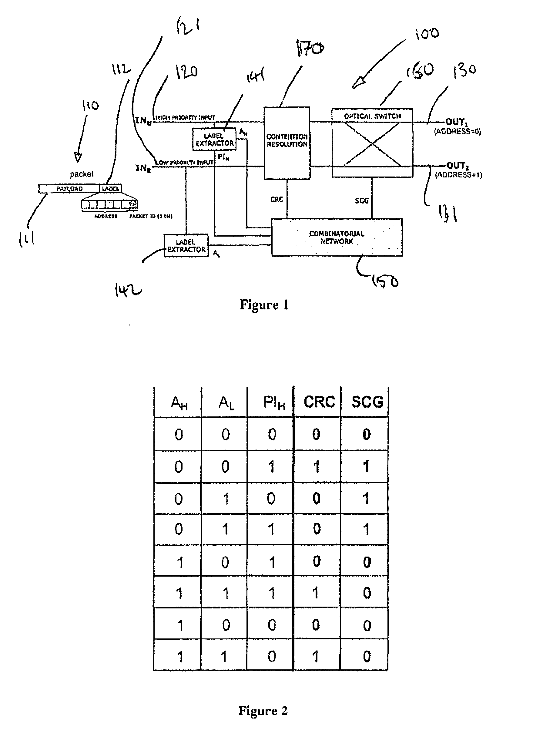
[0039]FIG. 1 illustrates the main components of an all optical switched optical node 100 for use, amongst other things, in an optical communication network. It is well known to route information along paths across an optical network. The information may be packetised, in which case sequential packets 110 of information are transmitted across the network which each comprise a payload 111 of data / information and an associated label 112. The label contains information which indicates the destination address of the associated packet.

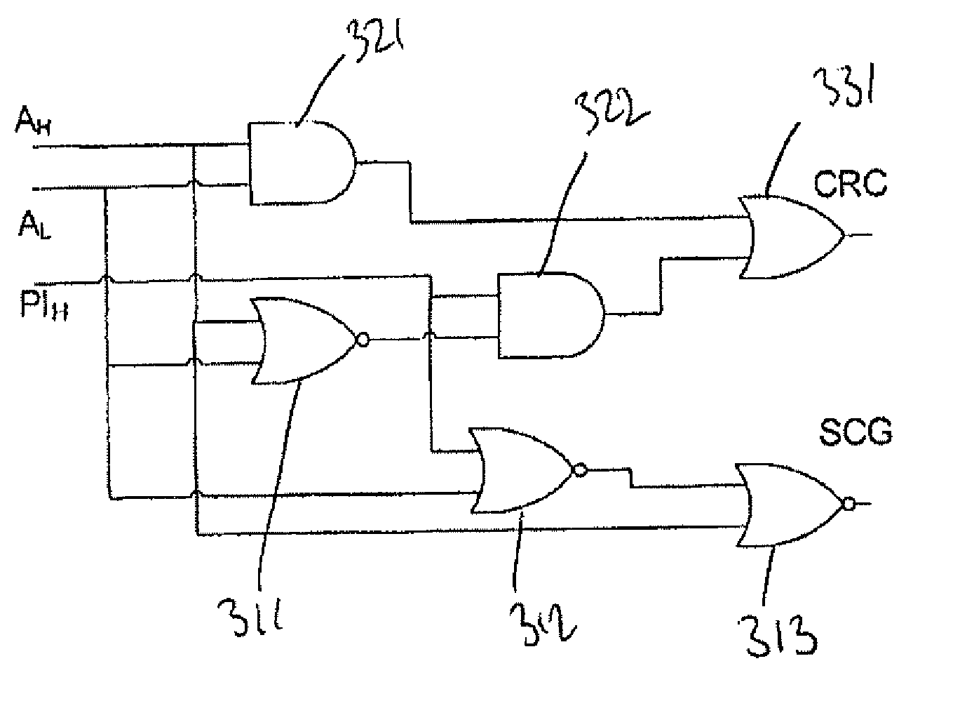
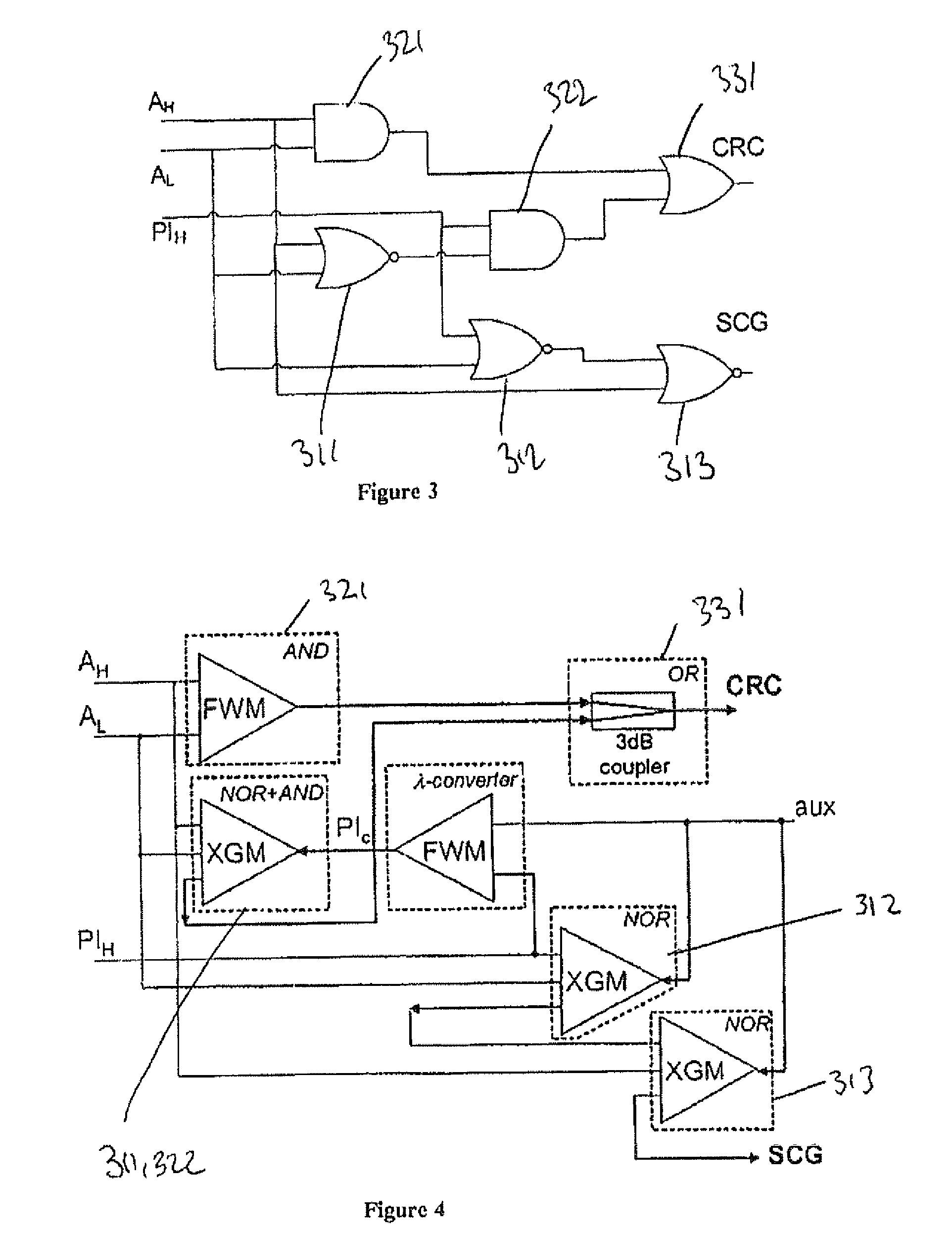
[0040]A 2×2 optical node has two inputs 120,121 and two outputs 130,131. Incoming information signals can be received at either input and can be received simultaneously in some cases. Upon receipt the information is stripped out of the labels by respective label extractors 141,142 to give destination addresses and a priority is assigned. The first input port in this example is given a higher priority than the other, so all signals it receives are considered ...


PUM

PropertyMeasurementUnit
optical domainaaaaaaaaaa
timeaaaaaaaaaa

Abstract

An optical processing circuit, such as a combinatorial network, comprises an arrangement of optical logic gates suitable for use in combination with a switched optical node of the kind having at least first and second input ports and two output ports, the node being configurable into either a cross or a bar configuration, and in which the optical processing circuit is arranged so as to receive at least three optical input signals which respectively comprise a packet identifier signal PIH which identifies whether or not a first input signal is present at the first input port of the switched optical node, the first input port being assigned a higher priority than the second input port, a first destination address AH indicating the output port of the switched optical node to which a first information carrying signal, received at the first input port, is intended to be passed, and a second destination address AL indicating the output port of the switched optical node to which a second information carrying signal, received at the second input port, is intended to be passed, and in which the processing circuit is configured to generate from these three optical input signals the following optical output signals: a contention resolution control (CRC) signal which has a first value if a routing conflict is present and a second if it is not; and a switch control generation (SCG) signal indicating whether the associated switched optical node is to be set in a cross or bar configuration.

Description

FIELD OF THE INVENTION[0001]This invention relates to improvements in optical circuits, in particular to an all optical processing circuit for conflict resolution and switch configuration in a 2×2 optical node. It is especially suited for use in conflict resolution and routing in a node of an optical communications network or optical computers.BACKGROUND OF THE INVENTION[0002]Optical 2×2 switches are known which have two input ports and two output ports and which are configurable in either a cross or a bar configuration. When set in the bar configuration, a signal received at a first input port IP1 is connected to a first output port OP1 and a signal received at the second input port IP2 is connected to a second output port OP2. When in the cross configuration the signal at the first input port IP1 is instead connected to the second output port OP2 and likewise the signal at the second input port IP2 is connected to the first output port OP1. This functionality enables information a...

Claims


Application Information

Patent Timeline
Patent Type & Authority Applications(United States)
IPC IPC(8): G02F3/00H04B10/27H04B10/291
CPCH04Q11/0005H04Q11/0066H04Q2011/0015H04Q2011/002H04Q2011/0058H04Q2011/0041H04Q2011/005H04Q2011/0052H04Q2011/0039G02F3/00
Inventor BOGONI, ANTONELLAPOTI, LUCASCAFFARDI, MIRCO
Owner TELEFON AB LM ERICSSON (PUBL)
Why Eureka
Try Eureka