Memory device, memory system having the same, and programming method of a memory cell

a memory cell and memory system technology, applied in the field of memory devices and memory systems having the same, can solve the problems of long programming time, inability to program or erase the entire block of resistive memory cells at the same time, etc., and achieve the effect of fast execution of program speed

Inactive Publication Date: 2010-08-26
SAMSUNG ELECTRONICS CO LTD
View PDF28 Cites 24 Cited by
  • Summary
  • Abstract
  • Description
  • Claims
  • Application Information

AI Technical Summary

Benefits of technology

[0005]It is therefore a feature of an embodiment to provide a memory device that enables fast execution of a program speed, a semiconductor system having the same, and a method of programming a memory cell.

Problems solved by technology

An entire block of resistive memory cells cannot be programmed or erased simultaneously, as this would require too large a drive current.
However, this results in a long programming time.

Method used


Image

  • Memory device, memory system having the same, and programming method of a memory cell
  • Memory device, memory system having the same, and programming method of a memory cell
  • Memory device, memory system having the same, and programming method of a memory cell

Examples


Embodiment Construction

[0036]Korean Patent Application No. 10-2009-0016330, filed on Feb. 26, 2009, in the Korean Intellectual Property Office, and entitled: “Resistive memory device, memory system including same, and programming method of the same,” is incorporated by reference herein in its entirety.

[0037]Exemplary embodiments will now be described more fully hereinafter with reference to the accompanying drawings; however, they may be embodied in different forms and should not be construed as limited to the embodiments set forth herein. Rather, these embodiments are provided so that this disclosure will be thorough and complete, and will fully convey the scope of the invention to those skilled in the art. Like reference numerals refer to like elements / features throughout the specification.

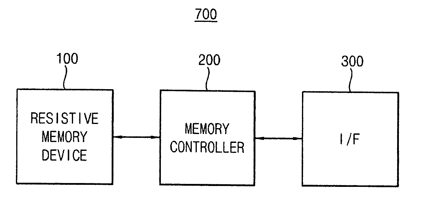
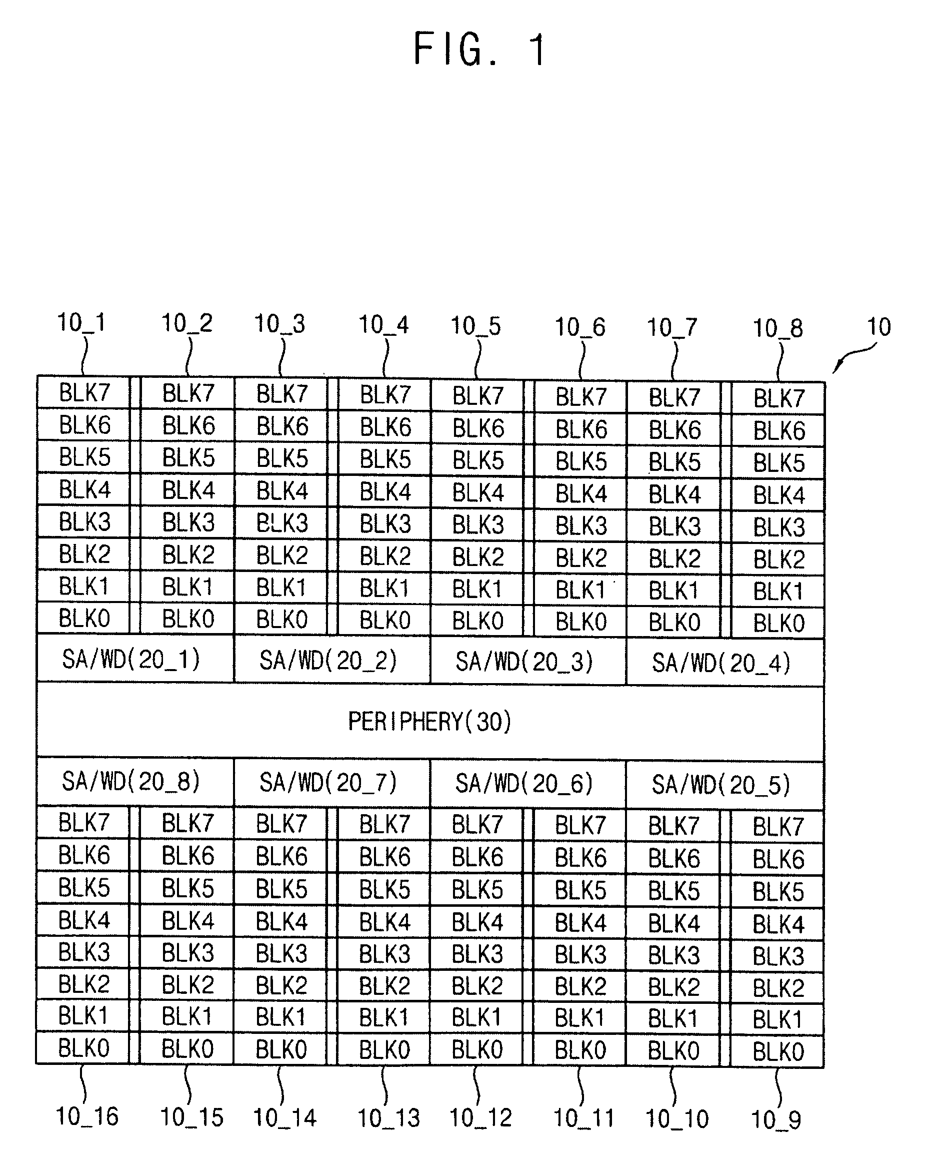
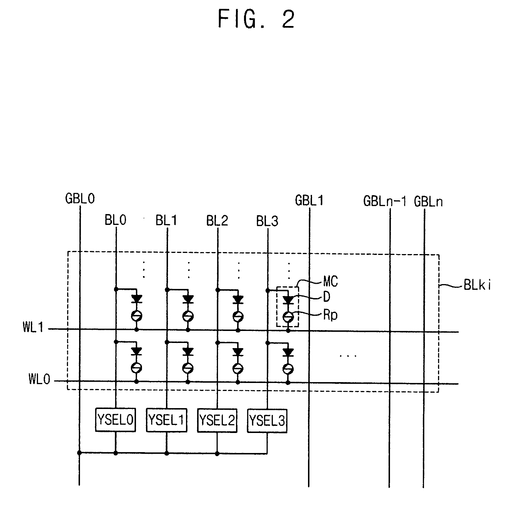
[0038]Hereinafter, embodiments of the invention will be described using a phase change random access memory device (PRAM) example. However, it will be apparent to those skilled in the art that embodiments may be appli...


PUM


Abstract

A memory device includes an array of resistance change memory cells divided into a first memory block including a first selected memory cell of a first plurality of memory cells and a second memory block including a second selected memory cell of a second plurality of memory cells, and sensing and writing circuitry configured to simultaneously activate a line connected with the first and second selected memory cells. The first and second selected memory cells may be written by iteratively applying a level-controlled write signal to memory cells not having a programmed state equal to the write data until a verify-read operation indicates respective programmed states for the first and second selected memory cells are equal to the write data.

Description

1. FIELD[0001]Embodiments relate to a semiconductor device, and more particularly, to a semiconductor device which enables fast execution of a program speed, a semiconductor system having the same, and a method of programming a memory cell.2. DESCRIPTION OF THE RELATED ART[0002]Memories are divided into volatile memories and non-volatile memories. Dynamic random access memories (DRAMs) and static random access memories (SRAMs) are volatile memories, while and flash memories, resistive memories, and phase change memories are non-volatile memories. The resistive memory uses a resistance value of a memory device to store one or more bits of data.[0003]An entire block of resistive memory cells cannot be programmed or erased simultaneously, as this would require too large a drive current. Accordingly, a block of such memory cells is programmed sequentially by applying a series of program pulses to respective cells. However, this results in a long programming time.SUMMARY[0004]Embodiments...

Claims


Application Information

Patent Timeline
Patent Type & Authority Applications(United States)
IPC IPC(8): G11C11/00G11C8/00G11C7/10G11C7/00
CPCG11C11/56G11C11/5678G11C13/0004G11C13/0061G11C13/0064G11C13/0069G11C2213/79G11C2013/0088G11C2013/0092G11C2211/5622G11C2211/5642G11C2213/72G11C2013/0076G11C13/0002G11C13/0007G11C11/15G11C13/00G11C13/02G11C16/12
Inventor KIM, HO-JUNGPARK, CHUL-WOOKANG, SANG-BEOMCHOI, HYUN-HO
Owner SAMSUNG ELECTRONICS CO LTD
Why Eureka
Try Eureka