Semiconductive rubber belt, and process for producing the same
a semi-conductive rubber and belt technology, applied in the direction of non-metal conductors, conductors, transportation and packaging, etc., can solve the problems of uneven formed images, inability to control the intensity of the transferring bias, and inability to solve the semi-conductive rubber belt. , to achieve the effect of even at a high level, even molecular orientation degree, and reduced unevenness of molecular orientation degr
Active Publication Date: 2010-09-16
NITTA CHEM IND PROD CO LTD
View PDF2 Cites 3 Cited by
- Summary
- Abstract
- Description
- Claims
- Application Information
AI Technical Summary
Benefits of technology
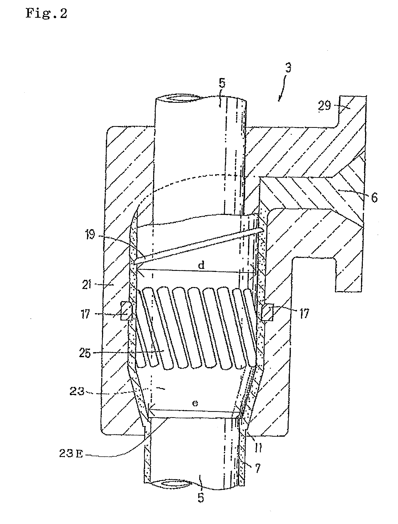
[0023]In the process for producing a semiconductive rubber belt, it is preferred that the ratio between the maximum outside diameter d of the inner cylinder section and the outside diameter e of a discharging opening in the section (the die contraction ratio) satisfies the following: 0.2≦e/d≦0.8, and further the shift speed of the cylindric
Problems solved by technology
When the electric resistance of the rubber belt is varied, formed images may become uneven.
Accordingly, ordinary manners of the tube extrusion molding process have a problem that weld lines are formed at intervals in the “belt circumferential direction” orthogonal to the width direction of the belt so that the electric resistance of the resultant semiconductive rubber belt is varied in the belt circumferential direction.
When the
Method used
View moreImage
Smart ImageViewing Examples

Examples
 PUM
| Property | Measurement | Unit |
|---|---|---|
| Electrical resistivity | aaaaa | aaaaa |
| Diameter | aaaaa | aaaaa |
| Electrical resistance | aaaaa | aaaaa |
Abstract
An object of the present invention is to provide a semiconductive rubber belt wherein a variation in the electric resistance is decreased, in particular, in the belt circumferential direction so that high-quality images can be formed, and a process for producing the same. In order to achieve the object, in a case where on any single straight line extended in the belt circumferential direction, the maximum value of the molecular orientation degree MOR-C of the semiconductive rubber belt, the minimum value thereof, and the average thereof are set to satisfy a specified relationship.
Description
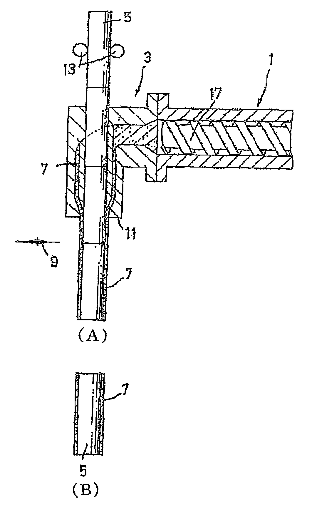
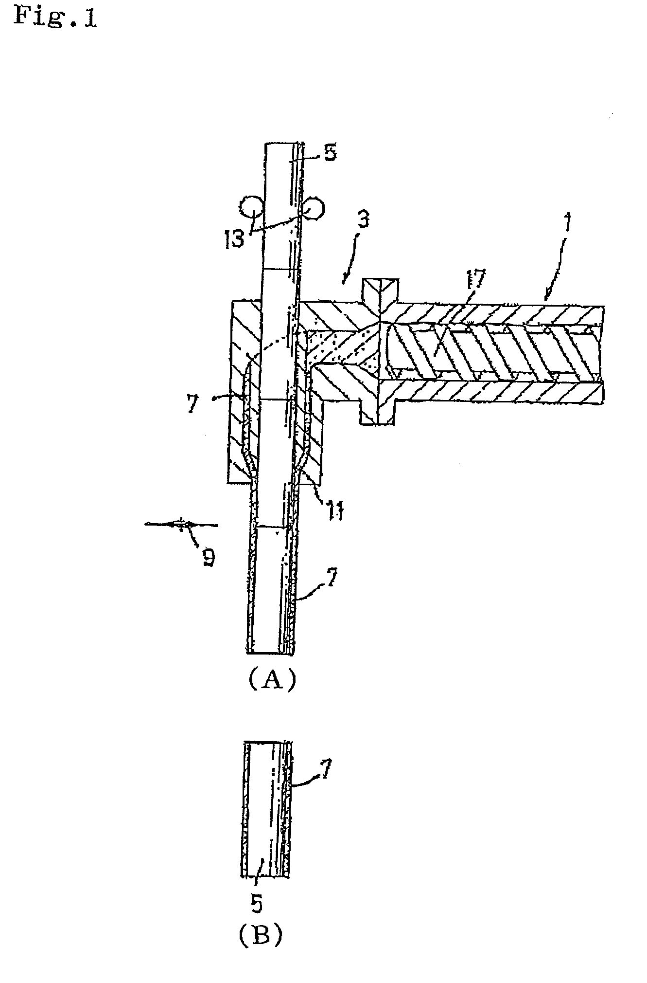
BACKGROUND OF THE INVENTION[0001]1. Field of the Invention[0002]The present invention relates to a semiconductive rubber belt used in a transferring section or the like in an image forming apparatus based on electrostatic photography, such as a copying machine, a printer, or a facsimile machine; and a process for producing the same.[0003]2. Description of Related Art[0004]The semiconductive rubber belt used in a transferring section or the like in an image forming apparatus is generally a belt containing a conductive filler, such as graphite or carbon black, and having a volume resistivity adjusted to the range of 104 to 1012 ohm-centimeters (Ωcm). The range of the volume resistivity is generally in the so-called semiconductive range. In this range, the electric resistance of the semiconductive rubber belt tends to vary in accordance with a slight variation in the amount of the filler that is added to the belt. When the electric resistance of the rubber belt is varied, formed images...
Claims
Login to View More Application Information
Patent Timeline
 IPC IPC(8): H01B1/12B29C47/00B29C48/157B29C48/09B29C48/151B29C48/34
CPCB29C47/0023B29C47/021Y10T428/24942B29K2021/00Y10T428/1386B29C47/028B29C48/09B29C48/151B29C48/157
Inventor NAKAGAWA, TAKAHIRO
Owner NITTA CHEM IND PROD CO LTD
Features
- R&D
- Intellectual Property
- Life Sciences
- Materials
- Tech Scout
- Unparalleled Data Quality
- Higher Quality Content
- 60% Fewer Hallucinations
Learn More Browse by: Latest US Patents, China's latest patents, Technical Efficacy Thesaurus, Application Domain, Technology Topic, Popular Technical Reports.
© 2025 PatSnap. All rights reserved.Legal|Privacy policy|Modern Slavery Act Transparency Statement|Sitemap|About US| Contact US: help@patsnap.com