

Semiconductor device and method of manufacturing the same
- Summary
- Abstract
- Description
- Claims
- Application Information
AI Technical Summary
Benefits of technology
Problems solved by technology
Method used
Image

Examples
second embodiment
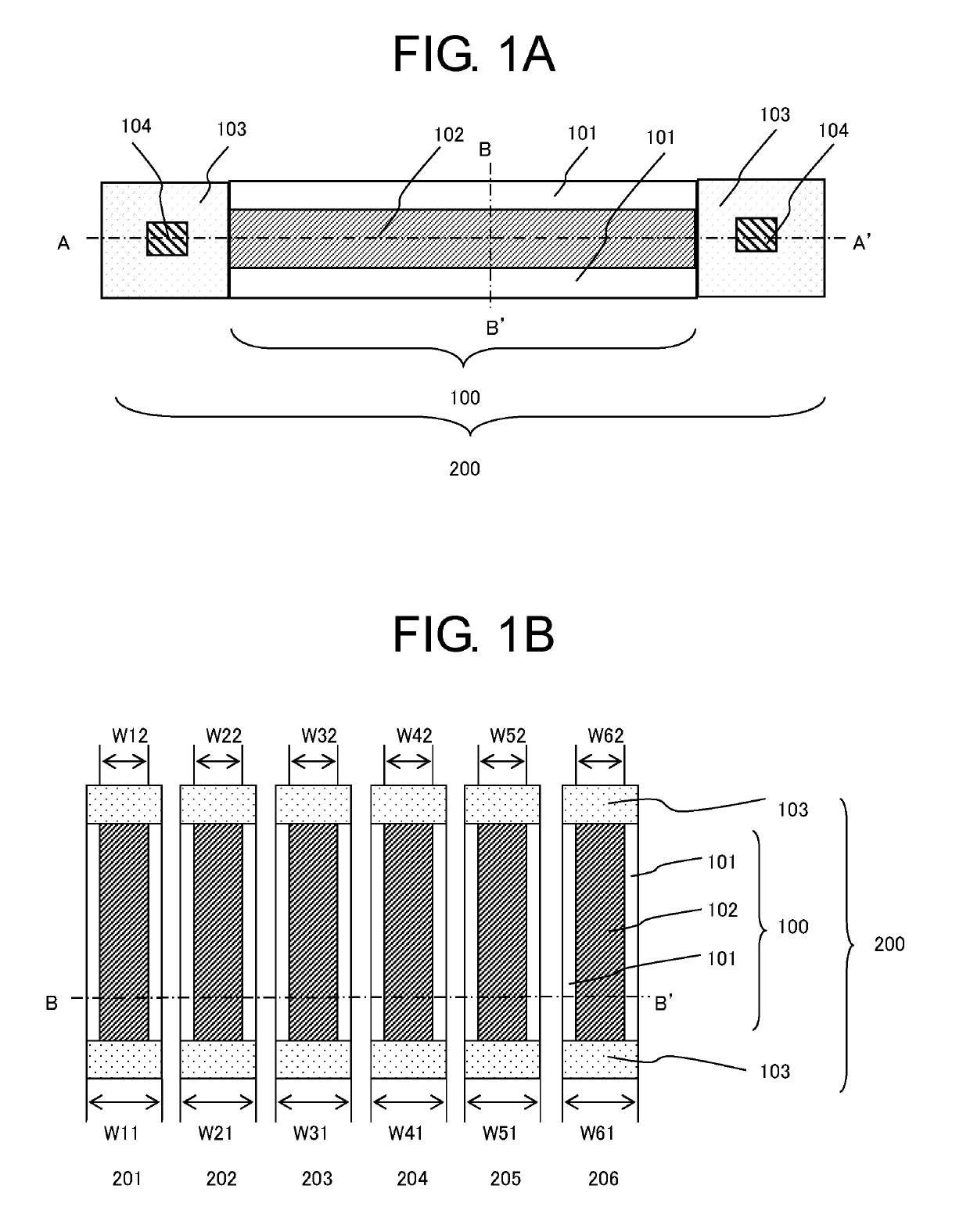
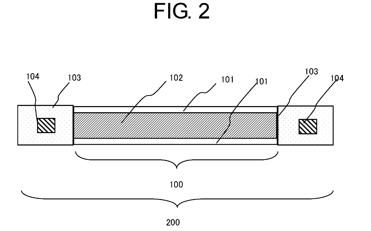
[0034]FIG. 2 is a plan view of a thin film resistor of a semiconductor device according to the present invention in which the width of the first high-resistance regions 101 is reduced due to the processing variation. The resistance of the entire thin film resistor is defined by a combination of the first high-resistance regions 101 and the second high-resistance region 102. The sheet resistance of the first high-resistance regions 101 is set to be 10 times or more higher than the sheet resistance of the second high-resistance region 102. As illustrated in FIG. 2, even if the width of the first resistance regions 101 is reduced due to the processing variation, an influence caused by the reduction in width of the first high-resistance regions 101 can therefore be suppressed to be smaller than the conventional thin film resistor in which the entire thin film resistor is formed of the second high-resistance region 102.
[0035]In conventional thin film resistors, for example, when the enti...
first embodiment
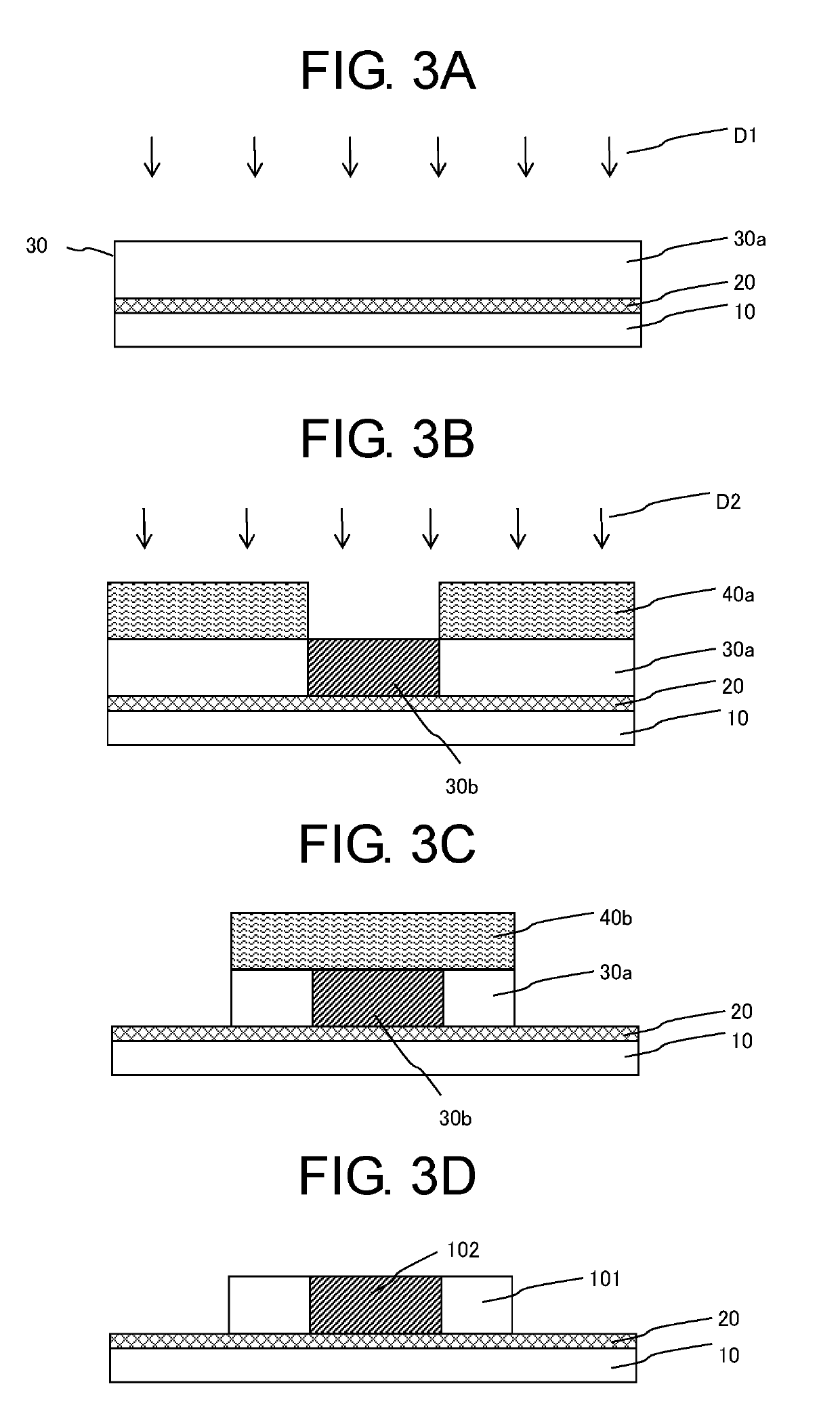
[0037]FIG. 3A, FIG. 3B, FIG. 3C, FIG. 3D, and FIG. 4 are sectional views for illustrating a manufacturing process for the thin film resistor of the semiconductor device according to the present invention. FIG. 3A, FIG. 3B, FIG. 3C, and FIG. 3D are sectional views taken along the transverse direction (B-B′ direction) of FIG. 1A, and FIG. 4 is a sectional view taken along the longitudinal direction (A-A′ direction) of FIG. 1A.
[0038]As illustrated in FIG. 3A, an insulating film 20 having a thickness of from 2,000 Å to 8,000 Å is deposited on a semiconductor substrate 10, and then, a non-doped polysilicon film 30 having a thickness of from 500 Å to 2,000 Å is further deposited. Next, P-type impurities such as BF2 are ion-implanted (ion implantation D1) into the polysilicon film 30 to form the first impurity region 30a. When the first impurity region 30a is a non-doped polysilicon film, the ion implantation D1 may be omitted.
[0039]Next, as illustrated in FIG. 3B, a resist pattern 40a is ...
PUM
 Abstract
Description
Claims
Application Information